Yukinori Ono, and Akira Fujiwara
Physical Science Laboratory
Complementary metal-oxide-semiconductor (CMOS) technology is now approaching the physical limit of scaling where quantum mechanical effects manifest due to the reduction of device size. On the other hand, several new devices are being explored to add functionalities based on quantum effects to silicon devices [1, 2]. Therefore, it is important to understand and control the quantum confinement effect to extend the functionality of silicon devices. Here, we report direct observation of electron subbands in thin silicon-on-insulator (SOI) metal-oxide-semiconductor field-effect transistors (MOSFETs) by tunneling spectroscopy [3].
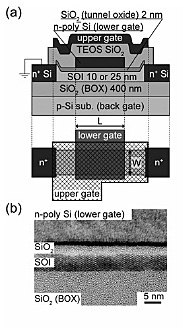
The observation of subbands was carried out in SOI-MOSFETs with 2-nm-thick
tunneling gate oxide [Fig. 1]. Figure 2(a) shows the tunneling current
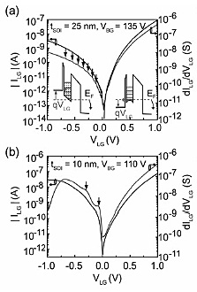
(ILG) and the derivative (dILG/dVLG) taken at 20 K for a sample with tSOI of 25 nm. Small peaks can be seen when VLG < 0. These characteristics are also seen for a device with a tSOI of 10 nm [Fig. 2(b)]. The appearance of these peaks only for negative
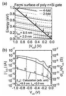
biases, which causes electron injection into the channel, and their tSOI dependence strongly indicate that they originate from the DOS structure of the thin SOI channel. To understand the observed structures quantitatively, we calculated the energies of the electron subbands in an SOI well for various electric field strengths. We found that the VLG at which the peaks appeared in the experiments is reasonably reproduced
by the subband edge of the fourfold valley [Fig. 3(a), (b)]. This is because
tunneling current is proportional to the DOS, and the magnitude of the
DOS for four-fold valleys is larger than that for two-fold ones, therefore,
four-fold valley subbands were clearly detected. We showed clear evidence
for the observation of a series of subband spectra in a structurally confined
SiO2/Si/SiO2 quantum well by tunneling spectroscopy.
[1] K. Uchida et al., J. Appl. Phys. 102 (2007) 074510.
[2] S. Saito et al., Jpn. J. Appl. Phys. 45 (2006) 679.
[3] J. Noborisaka et al., Appl. Phys. Lett. 96 (2010) 112102.
 |
 |
 |
||||||||
|
|
|