Hideaki Taniyama, and Masaya Notomi
Optical Science Laboratory, *NTT Photonics Laboratory
Photonic crystal (PhC) nanocavities, which exhibit a high cavity Q and an ultrasmall modal volume V, allow a strong light-matter interaction. As a result we can expect them
to provide the basis for very low power active devices. In particular,
the energy needed for all-optical switching based on the carrier-induced
resonance shift should be effectively reduced, because the required control
energy should be proportional to V/Q. In this study, we successfully achieved an extremely low switching energy and a fast switching time by combining InGaAsP, which exhibits a strong carrier-based nonlinearity, and an ultrasmall PhC nanocavity.
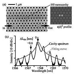
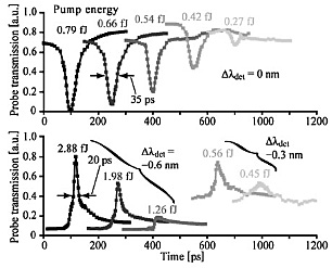
Figure 1(a) and (b) are a top-view image of the PhC structure and the transmission spectrum, respectively. The H0 nanocavity is formed by shifting two adjacent air holes in opposite directions. A computational calculation produced a modal volume V of only 0.025 µm3. Figure 2 shows the switching dynamics measured with a pump-probe technique.
When the probe pulse wavelength matches the modal peak, the probe pulse
transmission is abruptly switched off when the pump pulse temporally overlaps
the probe pulse. In contrast, the probe transmission is switched on at
shorter probe wavelengths. This is because carrier nonlinearity induces
a resonant blueshift. The minimum switching time window of 20 ps is attributed
to localized carrier generation and a fast carrier escaping from the cavity.
The switching energy with a contrast of 3 dB is only 0.42 fJ, which is
more than two orders of magnitude lower than that of previously reported
all-optical switches.
We showed that an InGaAsP-PhC nanocavity offers the possibility of realizing
an all-optical switch operating with ultrasmall energy, a fast response
time, and ultrasmall footprint integratability on a single chip. Other
PhC-based optical devices, such as optical memories, photo-detectors, and
modulators can also be achieved for chip-scale electronics-photonics interconnection.
This work was partly supported by CREST of Japan Science and Technology Agency.
[1] T. Tanabe et al., Appl. Phys. Lett. 87 (2005) 151112.
[2] K. Nozaki et al., Nature Photon. (in press).
 |
 |
|||||
|
|