In the past decade, chemical vapor deposition (CVD) growth of graphene has been emerged as a promising route to scale up the fabrication of graphene-based applications [1]. However, the CVD graphene samples are always polycrystalline, composed of single-crystalline domains having various in-plane rotations and related topological defects. These topological defects, especially grain boundaries, dominate the electrical and mechanical performance of large-scale CVD-grown graphene. Thus, an efficient method for elucidating the topological structure in CVD graphene is important for its fundamental research and potential technological applications in nanoelectronics and related fields.
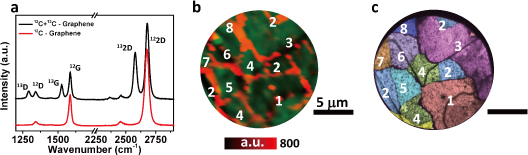
Here, for the first time we demonstrate an isotope labeling method to identify the topological defects in CVD-grown graphene by micro-Raman spectroscopy [2]. In a stepwise CVD process, the hydrogen and isotopic carbon sources are sequentially introduced after the standard growth of full-coverage monolayer graphene. Owing to the dual role of hydrogen in the catalytic reaction of graphene growth, the surface exchange of 12C-13C atoms occurs on a heated copper substrate. Taking the advantages of the distinct phonon energy between 12C and 13C lattice, we observed the coexistence of 12C- and 13C-graphene in an isotope-labeled graphene sample by Raman spectroscopy [Fig. 1(a)]. Moreover, as Fig. 1(b) shows, the 13C-rich regions form a pronounced network-like structure, isolating the 12C-graphene regions into micrometer-sized islands. The Raman characteristics of isotope-labeled graphene indicate that the carbon atom substitution is energetically favored along the grain boundaries of polycrystalline CVD graphene, which is further evidenced by low-energy electron microscopy (LEEM) characterization [Fig. 1(c)]. The carbon isotope labeling method provides a facile and effective way to characterize the topological defects in CVD-grown graphene, and also gives new insight for understanding the growth mechanism of graphene on copper catalyst.