LEAP Lasers Integrated on Si Waveguides
Data transfer is becoming a performance bottleneck in datacenters and high-performance computing. For further improvement, short-distance optical interconnects with large capacity and low energy cost are desired [1]. Since the required bandwidth is large in such interconnects, many photonic devices, which can operate with very small energy, need to be integrated with large bandwidth density [2]. In this context, we are studying photonic crystal (PhC) lasers integrated on Si waveguides, which enables large density owing to the large refractive index contrast. Here, we report the first continuous-wave (CW) operation of our PhC lasers on Si waveguides.
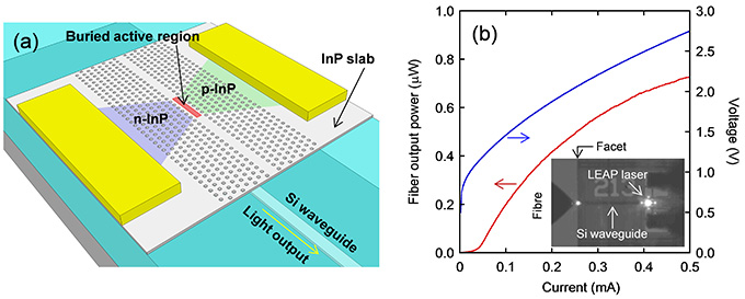
The device fabrication procedure was as follows. First, InGaAsP 6-quantum wells and InGaAs etch stop layers were grown on InP substrates and Si waveguides were formed by using silicon-on-insulator (SOI) substrates. SiO2 layers were deposited on InP substrates, and InP and Si substrates were bonded by oxygen-plasma-assisted bonding. After removing the InP substrate and InGaAs layer, we defined buried heterostructure patterns, followed by etching and regrowth to bury the active regions with InP. After fabricating the buried active region, a lateral p-i-n junction was formed by implantation and diffusion. Then we formed PhC air holes by electron-beam lithography and dry etching. Finally, electrodes were formed on top of the III-V slab. A schematic of a fabricated laser is shown in Fig. 1(a). From their structural feature, we call our lasers lambda-scale embedded active region PhC (LEAP) lasers.
We measured output light power and applied voltage as a function of injected current at 25°C, and the results are shown in Fig. 1(b). CW operation was successfully achieved with a threshold current of 42 μA. Maximum output power from the device was 0.72 μW at the lensed fiber at an injected current of 0.5 mA. The inset in Fig. 1(b) shows an infrared image of the device taken during measurements. From this image, we confirmed that the lasing light was successfully guided through the Si waveguides. We believe this achievement is an important step towards realizing short-distance, large-bandwidth-density optical interconnects.
- [1] A. Benner, Proc. OFC Tutorial (2012).
- [2] Y. Arakawa et al., Com. Mag. IEEE, 51, 72 (2013).
|
| Fig. 1. (a) Schematic of LEAP lasers fabricated on Si waveguides. (b) L-I-V characteristic and infrared image of the device. |