ü@
Hiroki Hibino1 and Kouta Tateno2
1Materials Science Laboratory, 2Optical Science Laboratory
ü@Au-Si alloy islands arranged at atomic steps were obtained by depositing Au on Si(111) at high (ü`700üÄ) and then low (ü`400üÄ) temperatures. Their size and density were controlled by monitoring the island formation in-situ in real time using low-energy electron microscopy. After the Au-Si alloy island formation, the samples were removed from UHV to air and introduced into the metal organic vapor phase epitaxy reactor without any special treatments. We found that there are three aspects to the growth of vertical GaP nanowires on Si(111): co-supply of trimethylgallium and PH3, two growths at different temperatures, and a low PH3 flow rate.
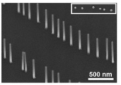
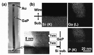
ü@Figure 1 shows a scanning electron microscopy (SEM) image of vertical nanowires self-arranged in lines with the length of several micrometers. The one-dimensional alignment of the wires proves that the Au-Si alloy islands arranged at the steps can be used as catalysts for nanowire formation. The SEM images also show that the wires have a fairly constant length and diameter. Figure 2 shows cross-sectional transmission electron microscopy (TEM) images and energy-dispersive X-ray spectroscopy (EDS) mappings of a GaP nanowire. There are no apparent defects passing through the nanowire/substrate interface, which is a promising feature for the integration of III-V semiconductor photonics into Si electronics.
ü@Our approach to control the size and position of nanowires does not involve any "top-down" lithographic techniques; it is a pure "bottom-up" self-assembly method. Self-assembly has potential advantages of low cost, large scale, high quality, and so on, but there still remain lots of problems to be solved, especially in the controllability of the size and position of nanostructures. We hope that our approach will contribute to establishing self-assembled nano-device fabrication methods.
[1] H. Hibino and Y. Watanabe, Surf. Sci. 588 (2005) L233.
[2] K. Tateno, H. Hibino, H. Gotoh, and H. Nakano, Appl. Phys. Lett. 89 (2006) 033114.
ü@
 |
 |
|||||
|
ü@ü@ |
|