Materials Science Laboratory
AlGaN/GaN high-electron mobility transistors (HEMTs) are being developed extensively for RF high-power applications. However, the output power of AlGaN/GaN HEMTs is limited by the thermal conductivities of the substrate materials. Among all materials, single-crystal diamond has the highest thermal conductivity of 〜 22 W/cmK. Therefore, diamond is expected to be the ideal substrate for high-power devices. However, due to the difference in the crystal structures of nitride semiconductors and diamond, single-crystal nitride growth on diamond substrates is difficult. Recently, using (111) surface orientation, we have successfully grown single-crystal AlN (0001) layers on diamond substrates [1, 2].
Here, using the single-crystal AlN as a buffer layer, we epitaxially grew
the AlGaN/GaN HEMT structure on diamond (111) substrate. As shown in Fig.
1, first, a 180-nm-thick AlN buffer layer was grown, followed by the growth
of 20-period AlN(3 nm)/GaN(17 nm) multi layers, a 600-nm-thick GaN layer,
a 1-nm-thick AlN spacer layer, a 30-nm-thick Al0.25Ga0.75N barrier layer, and a 4-nm-thick GaN cap layer. From X-ray diffraction measurements, we confirmed the single-crystal growth of the AlGaN/GaN HEMT structure. Next, we confirmed the formation of two-dimensional electron gas (2DEG) in the AlGaN/GaN heterostructure by Hall-effect measurement. The sheet electron density at room temperature was 1×1013 cm-2. On the other hand, the electron mobility at room temperature was 730
cm2/Vs.
A 3-µm-gate-length AlGaN/GaN HEMT on the diamond substrate showed
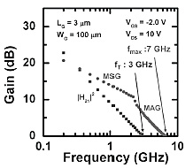
the maximum IDS of 220 mA/mm. Figure 1 shows the high-frequency small-signal characteristics.
From the frequency dependence of the current gain (|H21|2), maximum stable gain (MSG) and maximum power gain (MAG), the cut-off
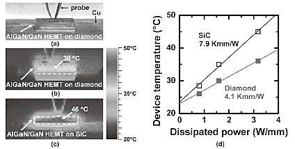
frequency (fT) of 3 GHz and maximum frequency of oscillation (fmax) of 7 GHz were obtained. Then, we compared the device temperature of AlGaN/GaN HEMTs on diamond and SiC substrates under high-DC-power operation. Figure 2(a) shows the setup for measuring the device temperatures. Figures 2(b) and (c) show the temperature distributions from the side of the AlGaN/GaN HEMTs on the diamond and SiC substrates at a dissipated power of 2 W (3.2 W/mm). The device temperature at 2 W increased from 23 to 36ºC (temperature rise ΔT = 13ºC). On the other hand, on the SiC substrate, the device temperature increased from 23 to 46 ºC (ΔT = 23ºC). From the dissipated power dependence of the device temperature rise [Fig. 2(d)], we estimated the thermal resistance of the AlGaN/GaN HEMT on the diamond substrate to be 4.1 Kmm/W, which is about half of that on a SiC substrate (7.4 Kmm/W) [3]. The low thermal resistance for the AlGaN/GaN HEMT on the diamond substrate is attributed to the high thermal conductivity of the single-crystal diamond. These results show that AlGaN/GaN HEMTs on diamond are promising for high-frequency and high-power applications.
[1] Y. Taniyasu and M. Kasu, J. Cryst. Growth 311 (2009) 2825.
[2] K. Hirama, Y. Taniyasu, and M. Kasu, J. Appl. Phys. 108 (2010) 013528.
[3] K. Hirama, Y. Taniyasu, and M. Kasu, Appl. Phys. Lett. 98 (2011) 162112.
 |
 |
|||||
|
|