Optical Science Laboratory
High-Q nanocavities have been extensively studied recently because they
are considered key elements in low-power photonic devices and integrated
circuits. These high-Q nanocavities in photonic crystals were fabricated
by a combination of high-resolution electron-beam lithography and dry etching
techniques. However, this means that the photonic crystal device components
should be incorporated in the CAD data before the fabrication process begins.
It is difficult to add other components to photonic crystals once they
have been fabricated.
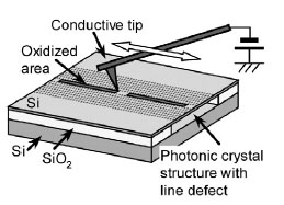
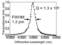
We propose employing the selective oxidation of silicon photonic crystals by using the scanning nanoprobe of an atomic force microscope (AFM) to form an ultrahigh-Q nanocavity in a line defect of a 2D Si photonic crystal slab as shown in Fig. 1 [1]. Selective anodic oxidation produces an ultrasmall oxide pattern on a Si surface if we apply a voltage between the probe's conductive tip and the target, which leads to local modification of the thickness and effective refractive index of a Si slab. This process is sometimes referred to as scanning-probe lithography (SPL) or AFM lithography. In this strategy, we utilize the fact that a very small spatial index modulation (Δn/n < 0.1 %) changes the mode-gap edge frequency of the modified area to create barrier regions, while the unmodified area retains its original modegap edge frequency [2]. We evaluate peak width of cavity resonance of a photonic crystal sample post-modulated by SPL and HF wet etching. As a result, an ultrahigh-Q (>1 million) nanocavities with a mode volume of 0.2 µm3 can be formed by employing scanning probe lithography on a pre-patterned line defect in a silicon photonic crystal as shown in Fig. 2. We confirmed that a photon lifetime of the cavity is around 1.25 ns. This is the first realization of ultrahigh-Q nanocavities by the post-process modification of photonic crystals. With this method, we can form an ultrahigh-Q nanocavity with controllable cavity parameters at an arbitrary position along a line defect. Furthermore, the fabricated nanocavity achieves ultralow power all-optical bistable operation owing to its large cavity enhancement effect. The threshold power for the bistable operation is close to the values obtained for conventional photonic crystal nanocavity devices. This demonstration indicates the possibility of realizing photonic integrated circuits on demand, where various circuit patterns are written with a nanoprobe on a universal photonic crystal substrate.
[1] A. Yokoo, T. Tanabe, E. Kuramochi, and M. Notomi, Nano Lett. 11 (2011) 3634.
[2] M. Notomi and H. Taniyama, Optics Express 16 (2008) 18657.
 |
 |
|||||
|
|