Tomonari Sato*, Ryo Takahashi*, and Masaya Notomi
Optical Science Laboratory, *NTT Photonics Laboratories
An optical random-access memory (o-RAM) will enable us to develop various
high-speed logic elements with a small power consumption [1], and is expected
to play a key role in future optical routers in which high-bit-rate optical
packets are processed without E-O/O-E conversion. A PhC nanocavity is a
possible candidate for an o-RAM because of its ultrasmall size, ultralow
power consumption, and large-scale integrability on a chip.
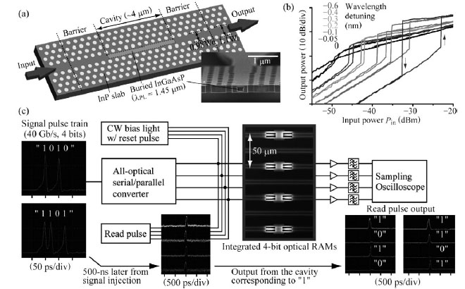
We achieved a novel buried heterostructure (BH) with which to form a PhC
nanocavity, as shown in Fig. 1(a), where an ultra-compact InGaAsP is buried
in an InP-PhC waveguide [2]. This structure allowed us to strongly confine
both photons and carriers, enabling a bistable behavior with very small
optical power, as shown in Fig. 1(b). Thus memory state switching between
the "on" and "off" states can be successfully obtained
with a combination of CW bias light and optical pulse input. Operation
power was only 30 nW, which is several orders of magnitude lower than of
the power required by previously reported o-RAMs.
To demonstrate the feasibility for integration, we fabricated a four-bit
memory array integrated in the same chip and demonstrated a four-bit RAM
operation as shown in Fig. 1(c). The 40-Gb/s data ("1101" or
"1010") were first spatially demultiplexed by an all-optical
serialto-parallel converter, and then stored in four different cavities.
Finally, the stored four-bit data were successfully read by injecting read
pulses after a buffering time of 500 ns. There has been no previous report
of integrated nanophotonics and our work is the first demonstration of
"Integrated o-RAM chip".
This work was supported by the National Institute of Information and Communications
Technology (NICT).
[1] M. Notomi et al., IET Circuits Devices & Systems 5 (2011) 84.
[2] K. Nozaki et al., Nature Photon. 6 (2012) 248.
 |
||
|