Broadening Light Emission at the Telecommunications Wavelengths by Material Engineering of Rare-Earth Compounds on Silicon
Erbium silicates (e.g. Er2SiO5 and Er2Si2O7) and erbium oxide (Er2O3) have great potential as optical amplifier materials in silicon photonics. Recent research has shown optical gain in waveguide erbium-doped amplifiers. However, the luminescence is limited by concentration quenching mechanisms, such as energy migration and up-conversion between Er3+ ions. Therefore, yttrium (Y), which has almost the same ionic radius as erbium (Y3+ of 0.9 Å, Er3+of 0.89 Å) and is optically inactive is incorporated to increase the luminescence efficiency of the Er ions in the silicates and oxides by forming ErxY2–xSiO5 and ErxY2–xO3. In addition, for further enhancement of the emission, ytterbium (Yb), with an ionic radius of 0.99 Å in Yb3+, has been incorporated in silicates and oxides. The incorporation of Yb effectively promotes the energy transfer from the Yb ions to Er ions, which results in high efficiency of the Er ion luminescence when pumped at a wavelength of 980 nm. In order for these materials to be used as gain media for optical amplifiers, they have to fulfill the requirement of broadband luminescence at the region of the C-band telecommunication transmission wavelengths (1530-1565 nm). Flat regions and broad peaks in the photoluminescence spectrum are required for broadband amplification. In this work, we grow ErxYb2–xSi2O7 and ErxYb2–xO3 crystalline mixtures on Si(111) substrates by RF-sputtering of Er2O3, Yb2O3 on Si and subsequent annealing in Ar atmosphere, and characterize their optical properties [1].
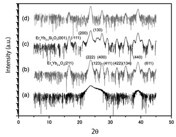
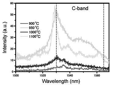
Thin films composed of polycrystalline ErxYb2–xO3 grains and crystalline ErxYb2–xSi2O7 layers were formed on a Si(111) substrate by RF-sputtering and subsequent thermal annealing in Ar gas ambient up to 1100oC. The films were characterized by synchrotron radiation grazing incidence X-ray diffraction (Fig. 1), cross-sectional transmission microscopy, energy dispersive X-ray spectrometry and micro photoluminescence measurements. In the annealed film of 950oC it is observed that the I15/2 - I13/2 Er3+ photoluminescence exhibits simultaneously maximum intensity and peak width at room temperature (Fig. 2). This effect satisfies the requirements for broadening the C-band of an optical amplifier on Si.
- [1]
- H. Omi, Y. Abe, M. Anagnosti, and T. Tawara, AIP Adv. 3 (2013) 042107.
 |
 |
|
|