Synthesis of Ultrathin Hexagonal Boron Nitride for Tunneling Applications
Production of atomically thin hexagonal boron nitride (h-BN) has considerably advanced in the past years given especially their synthesis is so much similar to the more popular graphene. Like graphene, the ability to control the number of layers is of fundamental interest as thin BN layers have the potential for several new applications such as a transport barrier for tunneling transistors and spintronics. Here, we report the growth of large-area, monolayer h-BN film on hetero-epitaxial Co film supported by a sapphire substrate.
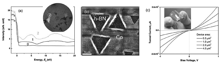
The synthesis was done using low-pressure chemical vapor deposition (LPCVD) method with ammonia-borane (NH3–BH3) or borazane used as BN precursors [1]. Our findings from growth evolution studies reveal that the growth of the monolayer h-BN film proceeds in triangular, oppositely oriented domains that are commensurate (1×1) to the underlying Co lattice (Fig. 1(b)). It is also inferred that these triangles are N-terminated and that the merging of the BN islands create defects at the domain boundary. The growth of h-BN appears to be self-limiting at a monolayer, with thicker domains only appearing in patches, presumably initiated between domain boundaries. Further, an alternative method for determining the number of layers of the synthesized h-BN film was developed by employing low-energy electron energy microscopy (LEEM). The measurement was taken directly after growth, and the number of layers can be determined from the reflectivity curve of the LEEM measurement (Fig. 1(a)), thus, information on the number of layers can be taken fast without the need for cross-section. Reflectivity measurements of the thicker h-BN films show oscillations resulting from the resonant electron transmission through quantized electronic states of the h-BN films, with the number of minima scaling up with the number of h-BN layers (Fig. 1(a)). First principles density functional theory calculations explain that the positions of oscillations are related to the electronic band structure of h-BN.
We also investigate the tunneling properties of the h-BN by fabricating metal/BN/metal devices on rigid and flexible substrates and compare the properties to exfoliated h-BN
(Fig. 1(c), inset) [2]. The measured current of the tunneling devices sandwiched by metal electrodes is linear around zero bias and increases exponentially at higher biases, a behavior consistent with direct tunneling (Fig. 1(c)). Further, from tunneling theory, we estimate the barrier height for tunneling to be ~2.5 eV, and the dielectric strength to be 3.78 ± 0.83 GVm–1, which are comparable to those of exfoliated monolayer BN. Our results demonstrate that CVD-grown BN can be a perfect alternative to exfoliated BN for tunneling applications, such as vertical transistors and spintronics, with an advantage of being available in a large area.
- [1]
- C. M. Orofeo, S. Suzuki, H. Kageshima, and H. Hibino, Nano Res. 6 (2013) 335.
- [2]
- C. M. Orofeo, S. Suzuki, and H. Hibino, J. Phys. Chem. C 118 (2014) 3340.
|
|
|
|