Applying Strain into Graphene - toward Strain Engineering of Graphene
The strain engineering of graphene is expected to make breakthroughs for graphene-based electronics. Graphene's high Young's modulus of 1 TPa and high elastic strain limit of 15% allow us to widely tune its electronic properties. However, applying strain under control is still challenging in experiments.
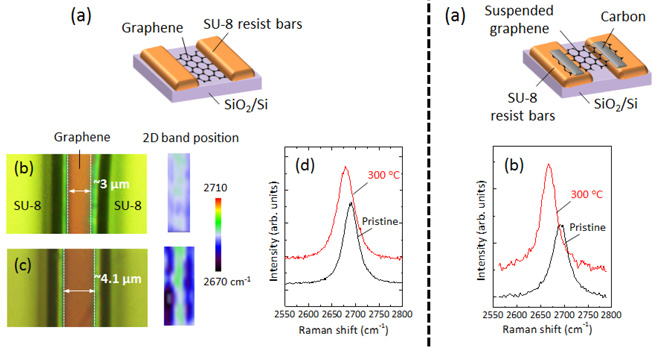
We thus investigated the strain in graphene induced by thermal shrinkage of SU-8 resist to establish a method for applying a strain with high controllability [1]. The SU-8 resist significantly shrinks ~10-20% when annealed at over 300oC, which is caused by dissociation of oxygen or hydrogen in SU-8. We studied two types of samples: grounded graphene (GG) [Fig. 1(a)], where two resist bars were deposited on graphene that had been transferred onto the substrate, and suspended graphene (SG) [Fig. 2(a)], where graphene was suspended between two bars of resist deposited on the substrate. In both samples, tensile strain is induced in graphene by shrinking the resist, where the resist pulls the graphene.
We first show results for GG samples. When we annealed a GG sample, the gap between the bars expanded [Fig. 1(b), (c)] and 2D peak position shifted to lower frequencies
[Fig. 1(d)]. These results indicate that the tensile strain was applied into graphene by shrinking the SU-8. From the 2D peak position maps [Fig. 1(c)], we also found that the applicable area of the shrinkage-induced strain is limited to near the resist (1-2 µm from it), which suggests that designing the resist deposition will allow us to locally control the strain in GG samples. Meanwhile, for SG samples, a larger tensile strain is induced. After annealing an SG sample, the 2D peak largely shifted to lower frequencies [Fig. 2(b)] and the amount of strain was three times larger than that for GG samples. We can conclude that a larger strain was induced because of the lack of adhesion between the graphene and substrate. We found that the configuration of SG will take full advantage of the large shrinkage of SU-8 for inducing a large strain, while GG allow us to induce a local strain. Our findings provide an avenue to the spatial control of graphene's mechanical, and consequently its electronic properties.
- [1] M. Takamura et al., Proc. 15th IEEE Int. Conf. on Nanotechnology, Rome, Italy, 33 (2015).
|
| (Left) Fig. 1. (a) A schematic of GG sample. Optical microscopy images and the corresponding Raman 2D peak position maps (b) before and (c) after annealing at 300oC. (d) Raman spectra before and after annealing. (Right) Fig. 2. (a) A schematic of SG sample. (b) Raman spectra before and after annealing. |