Er-Sc Silicate as an Optical Gain Material in Telecommunications Band
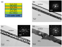
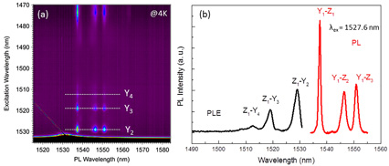
Photonic interconnects requires the development of new efficient and reliable on-chip optical device elements, including light sources, modulators, amplifiers, buffers, switches, and detectors. The realization of a silicon-based light source is considered to be one of the most challenging tasks. One of the possible solutions for the realization of silicon based light source is to use the emission from Er-silicates. Er silicates (Er2SiO5 and Er2Si2O7) have been attracting considerable attention as Er based materials for small size and high optical gain light source in silicon photonics integration, because they contain a higher Er density of 1022 cm−3 than Er doped Si-based materials. However, such a high concentration of Er results in up-conversion due to closely neighboring Er ions which limits the Er luminescence. Therefore, it is necessary to characterize and control the distance between Er ions in such Er silicates. An effective strategy for reducing this up-conversion is to incorporate yttrium (Y) cations into the structure, where they substitute Er ions in the silicate lattice and prevent neighboring Er ions from causing up-conversion due to the similar ionic radius between Y and Er. Scandium ions (Sc3+), on the other hand, are small (ionic radius = 0.75 Å) than erbium (Er3+) (ionic radius = 0.881 Å). Generally, this can result in enhancing the crystal field strength for Er doped silicates and oxides. In fact, Sc3+ ions in Er doped Sc silicate single crystals would increase the Stark-splitting of the thermally populated erbium ground state as well as that of other electronic energy levels of the silicates and thereby reduce re-absorption losses. In this work, we successfully synthesized a polycrystalline Er-Sc silicate and discilicate compounds in which Er and Sc are homogeneously distributed using RF-sputtering with multilayer Er2O3, Sc2O3, and SiO2 deposited on SiO2/Si (100) substrate and thermal annealing at high temperature [Fig. 1(Left)]. Photoluminescence (PL) measurements show the presence of ErxSc2-xSiO5 with an emission peak at 1528 nm for annealing from 900 to 1100oC, and ErxSc2-xSi2O7 with an emission peak at 1537 nm for higher annealing temperature. The PL intensity of the ErxSc2-xSi2O7 phase is five times stronger than that of the ErxSc2-xSiO5 phase at 1250oC. From PL excitation and PL spectra of ErxSc2-xSi2O7 thin film [Fig. 1(Middle), (Right)], we determined the energy levels of Er3+ ions in the silicates. Temperature-dependent PL of the ErxSc2-xSi2O7 phase exhibits a variation of the full-width at half-maximum (FWHM) from 1.1 to 2.3 nm. The narrow FWHM is due to the small ionic radii of Sc3+, which enhance the crystal field strength affecting the optical properties of Er3+ ions located at the well-defined lattice sites of Sc silicate.
- [1] A. Najar, H. Omi, and T. Tawara, Opt. Express 23, 7021 (2015).
|
|
| Fig. 1. (Left) Fabricated structures, (Middle) PLE color plot measured at 4 K obtained from the sample annealed at 1250oC. (Right) PLE and PL spectra at 4K. | |