Wavelength-scale All-optical Photonic Crystal Nanocavity Memory Operating at Nanowatt-level
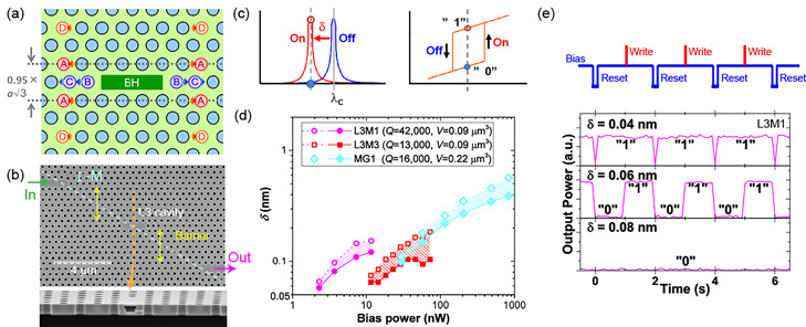
We are developing ultralow-power-consumption large-scale photonic integrated circuits on a chip using nanophotonic technologies. All-optical memory is one of the key devices. Since we need a considerably large memory, reducing power consumption is a crucial issue. We have realized an optical RAM with 30-nW operation using a wavelength-scale photonic crystal (PhC) nanocavity with a small buried heterostructure (BH) [1]. Here we describe a further one order of magnitude reduction of power consumption by employing a novel multi-hole-tuned three-missing-hole (L3) nanocavity with a BH placed at the cavity center [Fig. 1(a)] [2]. We used the same design as in [3], which enables large quality factor (Q) enhancement and multibit optical RAM operation [3]. In this study, a two-port filter design [Fig. 1(b)] was employed and Q was enhanced to 45,000 and 210,000 with and without the InGaAsP BH, where the latter is the record high value among all InP-based nanocavities. Two multi-hole-tuned BH-L3 cavities (L3LM, L3M3) were operated as an all-optical bistable memory as shown in Fig. 1(c) and compared to the operation of mode-gap-confined BH nanocavity (MG1) reported before [1]. As shown in Fig. 1(d), L3M3 that had Q comparable to MG1 decreased onset bias power to 10 nW thanks to the smaller mode volume (V) of the L3 nanocavity. Furthermore, L3M1 having much higher Q (42,000) exhibited onset bias power of 2.3 nW, which is nearly 1/13 of MG1’s, and the corresponding average number of photons in the cavity was only 0.1. Even at the 2.3-nW bias power, L3M1 operated with a very good "1"/"0" switching contrast [Fig. 1(e)]. This study paves the way for ultralow power consumption integrated photonic crystal devices and encourages the employment of multi-hole-tuned L-type nanocavities for fundamental and device studies.
- [1] K. Nozaki et al., Nature Photon. 6, 248 (2012).
- [2] E. Kuramochi et al., Appl. Phys. Lett. 107, 221101 (2015).
- [3] E. Kuramochi et al., Nature Photon. 8, 474 (2014).
|
| Fig. 1. (a) Design of systematically-tuned BH-L3. (Lattice constant (a): 426 nm. Shifts: 0.09a, 0.35a, 0.175a, and 0.045a for A, B, C and D. BH is InGaAsP.) (b) SEM image of L3 optical memory. (c) Schematics of all-optical bistable memory operation. (d) Relation between detuning (δ) and bias power for memory operation. (e) Input/output waveforms in memory operation at 2.3 nW bias power. |