An All-optical Packet Switch Realized by Using the Ultralow-powerOptical Bistability of a Nanocavity
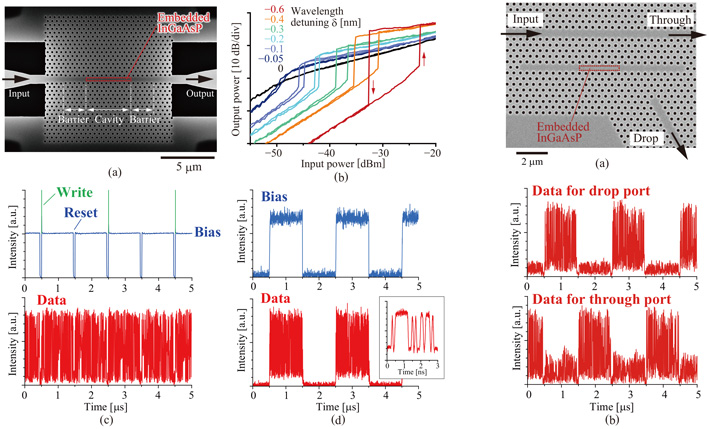
A tiny semiconductor nanocavity allows a strong light-matter interaction with a low-power optical input, and is used for various functional nanophotonic devices. We achieved a buried heterostructure with which to form a nanocavity, as shown in Fig. 1(a), where an ultra-compact InGaAsP is buried in an InP photonic crystal (PhC). This nanocavity allowed us to strongly confine both photons and carriers, thus enabling us to realize bistable behavior even with nW-level optical power, as shown in Fig. 1(b). Thus bistable switching between "on" and "off" states can be obtained by combining a CW bias light and an optical pulse input, and thereby make it possible to realize an all-optical memory. As an extended application, in this research, we demonstrated that it can work as an all-optical packet switch [1].
For this demonstration, a write pulse (100 ps wide, 13 fJ), a CW bias light (0.8 µW), and a reset pulse (50 ns wide) were injected to switch the bistable states, and the optical packet data (10 Gbit/s, 1 ns long, NRZ signal) to be switched were also injected, as shown in Fig. 1(c). As a result, we confirmed that the bistable states were switched with the output bias light, and gate switching for the optical packet was successfully achieved, as shown in Fig. 1(d). Furthermore, we also investigated a 1×2-port configuration, as shown in Fig. 2(a). This realized output-port-selective switching for the optical packet via bistable memory switching as well as gate switching, as shown in Fig. 2(b). The ultralow-power all-optical packet switch that we achieved is promising in terms of realizing a chip-scale high-speed photonic routing circuit that does not need E-O/O-E signal conversion.
- [1] K. Nozaki, A. Lacraz, A. Shinya, S. Matsuo, T. Sato, K. Takeda, E. Kuramochi, and M. Notomi, Opt. Express 23, 30379 (2015).
|
|
| Fig. 1. (a) Photograph of photonic crystal nanocavity. (b) Hysteresis curves on optical input/output characteristic. (c) Input optical waveforms. (d) Output waveforms showing the gate switching of optical packet data. | Fig. 2. (a) 1×2-port configuration of nanocavity. (b) Output waveforms showing the output-port-selective switching of optical packet data. |