Light-Field Driven Petahertz Electronic Oscillation with Attosecond Periodicity in GaN Semiconductor
High-speed photonic and electronic devices at present rely on radio-frequency (RF) electric fields to control the physical properties of a semiconductor, which limits their operating speed to terahertz (1012 Hz) frequencies. Using the electric field from light pulses, however, could extend the operating frequency into the petahertz (1015 Hz: PHz) regime. Here we demonstrate optical drive at 1.16-PHz frequency in the gallium nitride (GaN) semiconductor characterized by an isolated attosecond (10–18 Hz: as) pulse (IAP) [1].
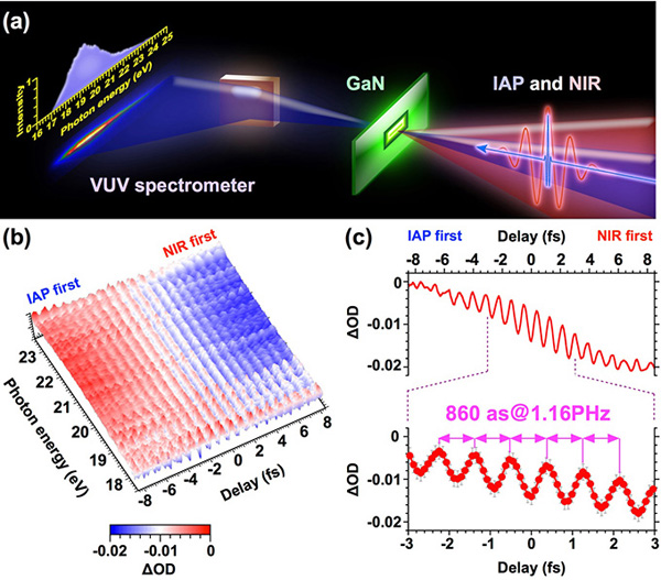
Figure 1(a) shows a schematic view of the transient absorption spectroscopy. The collinearly propagated IAP (660-as duration, 20.5-eV center photon energy [2]) and near-infrared (NIR) pulse (7-fs duration, 1.6-eV center photon energy, 1×10¹⁰ W/cm2) are focused onto stand-alone 102-nm thick GaN[0001] (bandgap energy: 3.4 eV). The NIR pulse induces ultrafast electronic interband polarization with the three photon process. Figure 1(b) displays the measured transient absorption trace. The trace shows the deviation of optical density (ΔOD) with and without the NIR pulse as a function of time delay. The coherent broadband IAP excites the superposition state of electrons in the valence band (VB) and conduction band (CB). Figure 1(c)
shows the electric oscillation with 860-as periodicity. The resultant frequency reaches 1.16 PHz, making this the first time the ultrafast electric dipole oscillation with PHz frequency is observed in Solid-state materials [1]. This study shows the potential of future PHz signal processing technology based on the semiconductor devices.
This work was supported by JSPS KAKENHI JP16H05987 and JP16H02120.
- [1] H. Mashiko et al., Nature Phys. 12, 741 (2016) : Featured on cover.
- [2] H. Mashiko et al., Nature Commun. 5, 5599 (2014) .
|
|
Fig. 1. Experimental setup and as transient absorption trace. (a) Schematic view of experimental setup. (b) Measured transient absorption trace of GaN. (c) The upper graph shows the integrated line profile structure for the photon energy region in Fig. 1(b). The bottom graph shows the profile in the shorter delay region. |