Bridging the Gap Between the Nanometer-scale Bottom-up and Micrometer-scale Top-down Approaches for Site-defined InP/InAs Nanowires
The field of microelectronics has been attempting to come to grips with the issue of miniaturization for decades as the demand for ever-smaller products puts pressure on manufacturers to make smaller components [1]. Despite the state-of-the-art Extreme Ultraviolet (EUV) photolithography technique, the low cost feature of the conventional UV photolithography is greatly advantageous over the high-cost EUV photolithography. This issue has opened the door to the development of other device fabrication methods [2]. Another competing method, self-assembly, relies on a bottom-up process that is driven energetically as the system reaches a lower energy state.
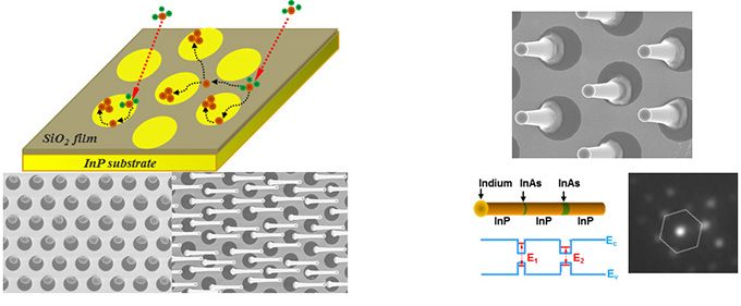
III-V compound semiconductor nanowires (NWs) are successful example of the bottom-up approach. For site-defined growth of III-V NWs with nanoscale diameter, top-down techniques like conventional photolithography are not feasible. This work presents a method that bridges the gap between the nanometer-scale bottom-up and micrometer-scale top-down approaches for site-defined NWs, which has long been a significant challenge for applications that require low-cost and high-throughput manufacturing processes [3]. We realized the bridging by controlling the seed indium nanoparticle position inside the open window through the optimization of the temperature and the pitch size. Site-defined InP NWs were then grown from the indium-nanoparticle array [Fig. 1(left)]. We demonstrated that the developed method can be used to grow a uniform InP/InAs axial-heterostructure NW array. The ability to form a heterostructure NW array makes it possible to tune the emission wavelength over a wide range through quantum confinement [Fig. 1(right)]. Successful pairing of a controllable bottom-up growth technique with a top-down substrate preparation technique greatly improves the potential for the mass-production and widespread adoption of this technology.
This work was supported by JSPS KAKENHI JP15H05735 and JP16H03821.
- [1] G. A. Brown et al., Mater. Today 7, 20 (2004).
- [2] B. D. Gates et al., Annu. Rev. Mater. Res. 34, 339 (2004).
- [3] G. Zhang et al., ACS Nano 9, 10580 (2015).
|
| Fig. 1. (Left) Schematic diagram of absorption, decomposition, surface diffusion, and accumulation of materials on the surface of SiO2 film and circular InP open windows. SEM images of indium seed particle array by self-assembly of indium adatoms and InP NWs grown from the particle array. (Right) SEM image of InP/InAs NWs with two InAs segments. Schematic structure and band diagram of the NW and spatial PL image with luminescence spots from InAs quantum disks. |