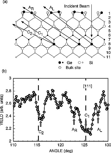
One or two atomic layers of Ge were embedded below 4 - 12 ML of Si overlayer grown with atomic layer precision by MBE. Since the ions scattered from embedded Ge layers can be distinguished from the signal of the Si substrate, the restricted scattering-blocking pairs are uniquely correlated with observed blocking profiles. In addition, the effect of thermal vibration can be minimized by choosing a distance between scattering and blocking atoms that is suitable for analysis. Therefore, we can observe a sharp and simple blocking profile of embedded Ge signals, and can determine the precise structure of the reconstructed surface. Figure 1 shows (a) the side view of the scattering geometry and (b) the corresponding MEIS blocking profile. We can see the extra dips (AL and AR) around direction. The origin of these smaller dips are assigned to the blocking effect caused by the surface dimer atoms. Therefore, we can determine the atomic displacements of the Ge-Ge dimer by analyzing blocking profiles.
Figure 2 shows the structural model of the Ge-Ge dimer on the Si(001) surface determined by the proposed method. We found that the dimer is asymmetric and the Ge-Ge bond length is 2.4 +- 0.1 A. We demonstrate that this method can determine the reconstructed surface structure in a more accurate way.
Fig. 1: MEIS blocking profiles for the embedded Ge signal.
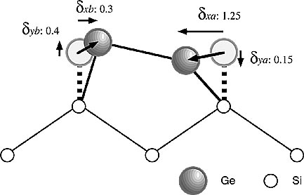
Fig. 2: The atomic displacements of the asymmetric dimer.