Quantum nanostructures, such as quantum point contacts (QPCs) or quantum dots, in high-In-content InxGa1-xAs have been attracting considerable attention for use in novel spintronic devices. By exploiting the strong spin-orbit interaction (SOI) in InGaAs, the electronic spin degrees of freedom can be manipulated through the SOI. For instance, electrons moving through QPC experience the selective spin-flipping process caused by SOI induced spin-splitting, which implies that InGaAs QPCs work as a spin-polarizer without the need of magnetic field. In addition to spintronic applications, InGaAs nanostructures are promising for the development of semiconductor/superconductor hybrid devices. Since high-In-content InxGa1-xAs (or InAs) forms low Schottky barriers (or no barrier for x > 0.77) against most metals, superconducting Cooper pairs can be effectively injected into InGaAs. As an example, superconducting quantum point contact, a counterpart of the semiconducting QPC, has been intensively investigated to realize a quantum bit using Andreev bound states or to observe Majorana fermions that are induced at the interface between an s-wave superconducting electrode and one-dimensional channel with strong SOI.
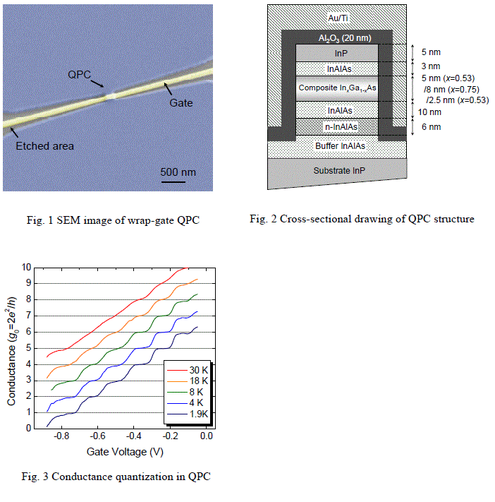
In this study, we improved fabrication technique for QPCs in an In0.75Ga0.25As/InAlAs two-dimensional electron gas heterostructure. The key challenge in realizing a well-behaved QPC is efficient electrostatic control of a one-dimensional channel using the gate electrode. The fabricated QPCs employ a 100-nm-wide mesa constriction and a gate electrode that wraps around the constriction for three-dimensional electric-field gating. Conformal aluminum-oxide growth by means of atomic layer deposition is employed to suppress gate leakage while minimizing the interface state density. Figs. 1 and 2 below show a scanning electron microscope image of the fabricated QPC and a schematic drawing of the cross section, respectively. The wrap-gate QPCs show clear conductance steps, demonstrating well-defined quantized transverse modes in the InGaAs-based one-dimensional channel, as shown in Fig. 3. This technique can be easily extended to the fabrication of quantum dots and superconductor/QPC/superconductor junctions, which opens up a novel approach for the studies of spin-related phenomena in InGaAs-based quantum nanostructures.