


Ultra-small and low energy consumption optical bit memory developed
- Long memory holding time of 150 nsec achieved in photonic crystal, toward integration -
NTT Basic Research Laboratories, in collaboration with NTT Photonic Laboratories, have developed an optical bit memory by using a small artificial periodic structure called a photonic crystal, and have achieved a memory holding time of up to 150 nsec which is 60 times longer than our previous record.
An optical memory with low power consumption has been realized by employing an InGaAsP photonic crystal. Its minimum bias light power is 40 μW, which is two orders of magnitude lower than conventional optical memories that employ optical bi-stable operation in semiconductor lasers.
This new memory is ultra-small and suited to integration. Its low power operation paves the way for the realization of a practical optical memory that can be applied to all-optical information processing, which transmits and processes optical digital data without changing it to electrical data. All-optical information processing is attracting attention because it is free from the limits on, for example, power consumption or operating speed imposed by information processing techniques.
This achievement will be presented at the international conference "Conference on Lasers and Electro-Optics" held from May 4, in San Jose, USA.
=> Photonic Nano-Structure Research Group
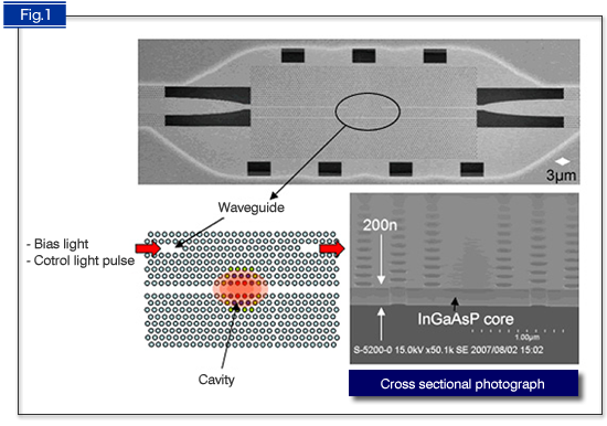
Fig. 1 Structure of InGaAsP photonic crystal
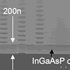
The photonic crystal used for the optical memory is a 200-nm-thick semiconductor crystal with 200-nm-diameter through-holes arranged at the triangular lattice position with a 420 nm period. The photonic crystal has a linear region that does not have through-holes that works as a waveguide. By slightly shifting (several nm) some of the through-holes that reside on both sides of the waveguide, part of the waveguide becomes thicker. The thicker region works as a cavity, which is the heart of the memory. InGaAsP has a larger optical nonlinearity, and in this respect, it has an advantage over Si. However, InGaAsP is harder to process than Si, and a high quality photonic crystal that confines light efficiently has been difficult to fabricate. The newly fabricated photonic crystal cavity exhibits a very large Q-value, which is an index of confinement strength. The maximum measured Q-value is 130000, and this is the largest value ever obtained. In addition to the large optical nonlinearity of InGaAsP, the realization of the high quality cavity led to optical memory operation with low energy consumption.
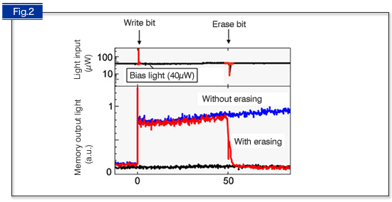
Fig. 2 Overview of memory operation
In the memory, the output light intensity is used as bit information under bias light irradiation. The initial state is defined as the state before the injection of control pulses. The bias light has taken to be slightly detuned from the resonant wavelength of the cavity and does not transmit the cavity yielding the low level output. This state is defined as the memory "OFF" state (black curve in figure). By injecting the write pulse, the refractive index of the cavity is changed due to the nonlinearity, and the cavity resonant wavelength is shifted toward the bias light wavelength. Correspondingly, the transmittance of the cavity becomes high yielding a high level output. This is the memory "ON" state. The "ON" state holds after the control pulse has passed through. This means the bit information has been correctly retained. The memory can also be erased by using an erase pulse. The maximum memory holding time of this device is 150 nsec. This is 60 times longer than a device that uses the Si for the photonic crystal, and it is long enough for optical RAM operation. Furthermore, the minimum bias light power for holding the bit data is 40 μW, which is nearly two orders lower than that for a conventional bi-stable laser optical memory.


