


World's first large-scale coupling of optical nanocavities generating slow light
- Step toward to the realization of multi-functional optical information processing using slow light -
NTT Basic Research Laboratories have realized a structure where optical nanocavities are coupled on a large scale on a chip for the first time in the world. Moreover, this structure has been used to reduce the propagation speed of an optical signal. The structure uses a photonic crystal, which is an artificial periodic structure with strong optical confinement effect, and the cavity is about the size of the wavelength of light. (Fig. 1)
A large-scale coupled structure of ultra-small cavities has a similar nature to the coupled atoms in a crystal, and because of this nature it is considered to be a superior medium that can reduce the propagation speed of light. However, it is technically difficult to couple many ultra-small cavities, and no high-quality large-scale coupled structure has yet been realized. NTT Basic Research Laboratories have produced an optical nanocavity with a confinement volume of 0.1 µm3 that is similar in size to the wavelength of light. The large-scale coupled cavity structure has been realized by using 200 nanocavities, and the fact that the structure has similar features to the coupled structure of atoms has been demonstrated for the first time anywhere in the world. The characteristics of the coupled cavity structure are significantly better than previously reported, and an optical signal pulse propagation speed of about 1/100 (1/170 at most) of the light velocity in air has been obtained (Fig. 2).
This achievement was published in the online express edition of the UK science journal "Nature Photonics" on November 23.
=> Photonic Nano-Structure Research Group
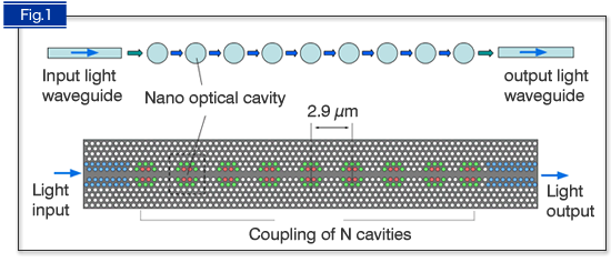
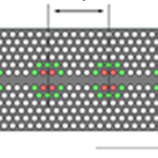
Fig. 1 Conceptual (top) and schematic (bottom) diagrams of a large-scale coupled cavity fabricated using a photonic crystal.
A photonic crystal is made from crystalline silicone with periodic holes each about 200 nm in diameter. Nanocavities were produced by slightly shifting the position of the colored holes in the figure, and coupling them to realize a large-scale coupled cavity structure.
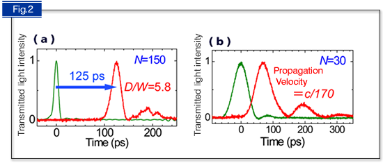
Fig. 2 Propagation measurement of an optical pulse in large-scale coupled cavities.
The red curve represents the optical pulse after it has passed through the coupled cavities, while the green curve represents a linear waveguide without coupled cavities used as a reference. (a) The red curve shows a 125 psec delay by comparison with the green reference curve. This delay is 5.8 times larger than the increased pulse width by passing through the coupled cavities. (b) Largest delay in propagation. The propagation speed is 1/170 of the light velocity in air.


