


World premier: Success in realizing all-optical RAM
- Stepping into all-optical network processing with ultralow power consumption and high processing speed -
NTT Basic Research Laboratories and NTT Photonics Laboratories have demonstrated a monolithically integrated optical random access memory (RAM) chip by employing an artificial structure called a photonic crystal, which confines light tightly in an extremely small region. The power consumption of the chip is 30 nW, which is more than 300 times less than the previous record. This new chip has made it possible to accumulate and transfer an optical signal without converting it to an electrical one. And it is expected to help increase the operating speed and reduce the power consumption of networking equipment such as routers.
We have fabricated an ultra-small optical memory with a nano-scale cavity made of a photonic crystal that we fabricated using an InP slab embedded with a tiny bulk InGaAsP region. This structure has the following important features. (1) It exhibits large optical nonlinearity due to the strong confinement of both light and carriers. (2) Generated heat can quickly escape from the cavity and the problem regarding the operational instability of the optical memory has been resolved. As a result, an extremely low power consumption of 30 nW has been achieved (1/300 of the former record) as well as a long memory holding time of 10 seconds.
We have also fabricated an optical RAM chip with monolithically integrated 4-bit memories. This is the first realization anywhere in the world of integrated multi-bit optical RAM operation.
This result was reported in the express online edition of "Nature Photonics" magazine on February 26.
=> Photonic Nano-Structure Research Group
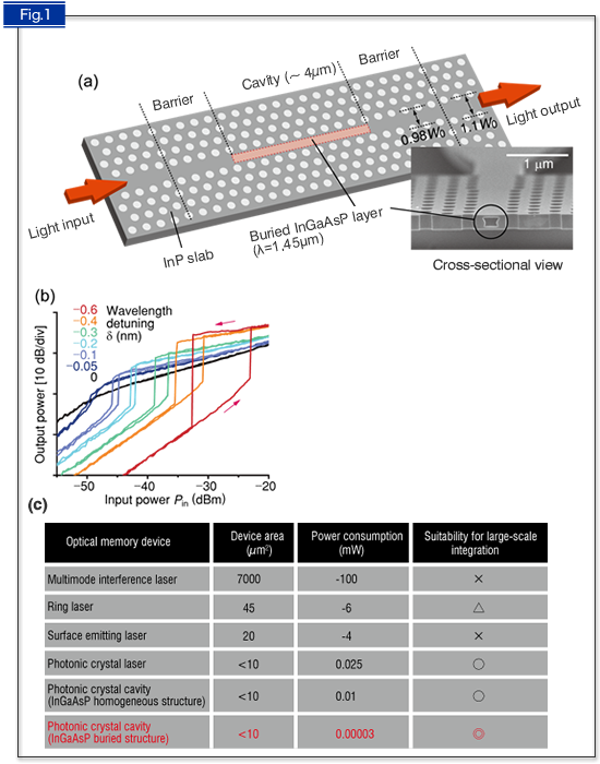
Fig. 1 Optical memory device using photonic crystal cavity
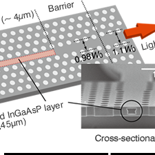
(a) Schematic diagram of the device. A tiny InGaAsP region is buried in the InP photonic crystal waveguide and it acts as a nano-scale cavity that confines both light and carriers. (b) Optical bistability characteristics for various amounts of wavelength detuning. Optical bi-stability has been observed that shows different output states when we increase and decrease the input light intensity. This phenomenon can be used to hold the state of an optical memory. (c) Comparison of performance for various types of optical memory. Our buried hetero cavity in a photonic crystal region has a much smaller operating energy and device size and is suitable for large-scale integration.
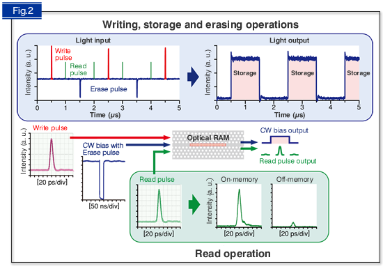
Fig. 2 RAM operation for optical data
When a write light pulse is injected, the bi-stable state changes to other states and increases the bias light output (write operation). The new state lasts until the injection of an erase pulse (storage, erase operation). Within the memory holding time, the written optical data is reproduced (read operation) by injecting the read pulse. Consecutive optical RAM operation has been demonstrated experimentally. Although the memory holding time is 1 microsecond in this figure, a 10-second or longer memory holding time has been confirmed.
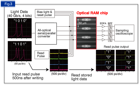
Fig.3 4-bit memory operation by the integrated optical RAM-chip
4-bit optical serial data of "1010" and "1101" were converted to parallel data by using an all-optical serial-to-parallel converter and the converted parallel data have been stored in an individual nano-cavity. We also injected a read pulse with a delay of 500 ns after writing into some of the cavities and we obtained a light pulse only from the cavities in which we had written the data. This shows the data have been output after the data light was stored in 500 nsec.


