


Development of a groundbreaking process for release of GaN-based thin-film devices from substrates
- Towards flexible LED, UV-sensitive high efficiency solar cell, and hybrid CMOS -
NTT Basic Research Laboratories (NTT-BRL) have succeeded in developing a novel process for release of GaN-based thin-film devices from substrates, where an extremely thin layer of boron nitride (BN) is grown between a sapphire substrate and the GaN-based thin-film device and works as a release layer. This technology facilitates a low-cost transfer of the resulting nitride structures (typically a few μm thick) to any other substrates. Accordingly, preparation of novel devices such as very thin light emitting diodes (LEDs), transparent solar cells sensitive only to UV light, and highly-functional hybrid CMOSs becomes possible. This achievement was published in the April 12th issue of the English science journal "Nature".
Background
GaN based semiconductors have been widely employed for the high-power electronic devices for wireless communications as well as for the visible light sources for illuminations and traffic signals. At present, these devices are fabricated by processing the GaN-based thin films together with single-crystalline substrates. Although the substrates (typically, 0.5 mm thick) are indispensable for the epitaxial growth and device fabrication processes, some potential applications of the thin-film devices have been hampered by the sterically-bulky substrates. Accordingly, a tremendous worldwide effort has been underway to release the thin-film devices alone and transferred them onto other materials.
Achievement
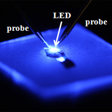
NTT-BRL has newly developed a technique of growing high-quality layered BN thin films on sapphire substrates and also growing high-quality GaN-based thin films on BN buffer layers. Since, in this structure, the cleavable BN plays the role of a release layer, one can mechanically detach the GaN-based thin-film devices from the sapphire substrates and transfer them to other substrates. This is named MeTRe (Mechanical Transfer using a Release layer) method. This development is achieved based on our well-matured growth technology for the nitride semiconductor thin films, which has been developed and accumulated in our laboratories. By using the MeTRe method, a thin film device can be released from a substrate without any deterioration in quality (Fig. 1) and can be attached to even flexible (e.g., plastic) substrates (Fig. 2). Further investigation is currently underway for applying this technology to wall/window/vehicle-attachable solar cells as well as for increasing the area of the transferrable thin film devices.
=>Thin-Film Materials Research Group
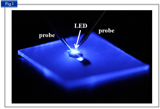
Fig. 1 Blue light electroluminescence from the transferred LED.
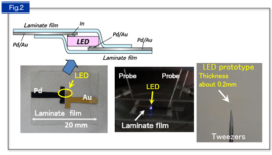
Fig. 2 LED wrapped with laminate films.
It has been demonstrated that the LED can be transferred to a flexible (e.g., plastic) substrate.


