


Over-100-bit Integrated Optical Memories Realized
- Big progress toward ICT with low power consumption -
NTT Basic Research Laboratories has realized an over-100-bit optical random access memory (RAM) *1 by integrating ultrasmall optical memories based on photonic crystal nanocavities*2, *3.
This device will enable ultrafast information processing via optical signals, which will reduce the increasing power consumption of information and communication technology (ICT).
This result will be published in the UK science journal "Nature Photonics" on 25th, May 2014.
=> Press Release
=> Photonic Nano-Structure Research Group
The energy consumption of ICT has been increasing year by year at an explosively accelerated pace, and it is thus strongly demanded to introduce novel technologies to reduce it drastically. As the bit rate goes up, the energy consumption of ICT becomes dominated by electric systems/instruments, such as routers and data centers. This is because the electrical signal processing becomes more energy-consuming when the bit rate goes up. The introduction of optical signal processing, which will not be constrained by the limitation of electronics, is expected to solve this forthcoming problem.
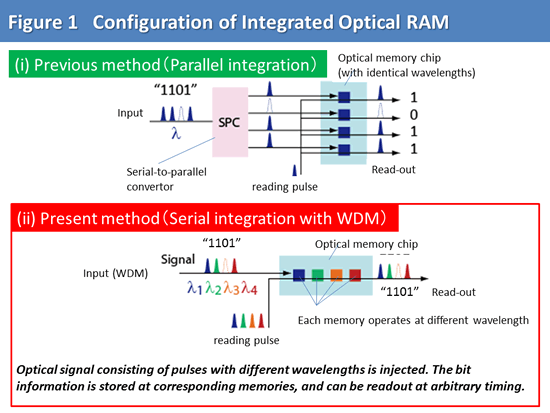
It is well known that RAMs play a key role in sophisticated information processing such as network routing, but previous optical memories are too large to integrate in a large scale. Hence, it has been thought that an optical RAM is one of the most difficult devices to realize in optical processing. In order to solve this problem, in 2012 NTT adopted an artificial material called a photonic crystal which is able to strongly confine light, and demonstrated four-bit optical memories with photonic crystal nanocavities by employing the parallel integration method shown in Fig.1(i). However, further large-scale integration was not achieved yet.
NTT Nanophotonics Center in NTT (Atsugi, Kanagawa), which is conducting fundamental research for large-scale optical integration and optical processing with low power consumption, has just succeeded in large-scale integration of over-100-bit optical memories with the wavelength division multiplexing (WDM) method *4, illustrated in Figure 1(ii), enabled by novel optical nanocavities (explained later in Fig. 5) based on a photonic crystal.
Since the integrated size of optical bit memories was four at largest prior to this, the achievement of over-100-bit optical memories announced here demonstrates a clear feasibility of realistic optical random access memories for optical processing. Furthermore, such large-scale optical integration of sub-micron optical devices has been achieved for the first time even other than memories, and therefore this achievement is an important big step toward full-fledged optical integration because this shows that we will be able to integrate a very large number of tiny optical devices in a single chip, in a similar way to integrate transistors in a chip.
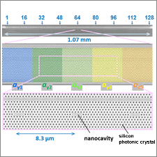
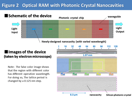
Figure 2 shows a schematic of the optical memory realized. Multiple optical memories whose operation wavelength slightly differs are integrated in a serial fashion, side coupled to a input/output optical waveguide. By appropriately choosing the wavelength, we are able to write and read a bit information of each cavity randomly. This configuration has been achieved by integrating over-100 nanocavities having different resonant wavelength in a silicon photonic crystal by the high-resolution nano-fabrication technology with accurate wavelength controllability. Owing to the unique property of photonic crystals, light is strongly confined in each cavity as a volume less than 0.1 m3, and all nanocavities are densely integrated with a period of approximately 8 µm3. Figure 3 and Figure 4 demonstrate that 105 optical memories can actually operate independently, whose detail is describe below.
Detail of memory operation
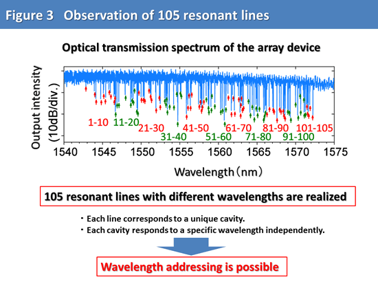
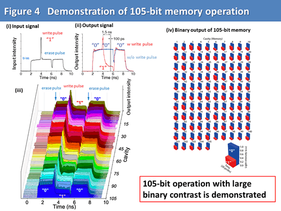
- As shown in Figure 3, the device shows 105 resonant lines (dips) which was observed by inputting broadband light into the device and measuring the output.
- The random access memory operation is achieved by inputting optical signals whose wavelength matches one of the resonant lines. A typical optical output from this device is shown in Figure 4(i), which was obtained when the optical input shown in Fig. 4(ii) was injected at one of the resonant lines. As shown, the output initially at the “0” level was switched to the “1” level after injecting a writing pulse. Since the “1” level was preserved even after the writing process, it shows that the information was properly stored. Finally, the output returned to the “0” level after the easing pulse, which shows that the stored information was erased. Figure 4(iii) summarized results for all 105 bits, which clearly shows that the operation similar to Fig. 4(ii) was indeed realized for all bits.
- Figure 4(iv) shows temporal outputs from all 105 bit memories when information of "0" or "1" was written. This result clearly demonstrates that the binary information is appropriately stored in all 105 bits with sufficiently high contrast.
Technical Features
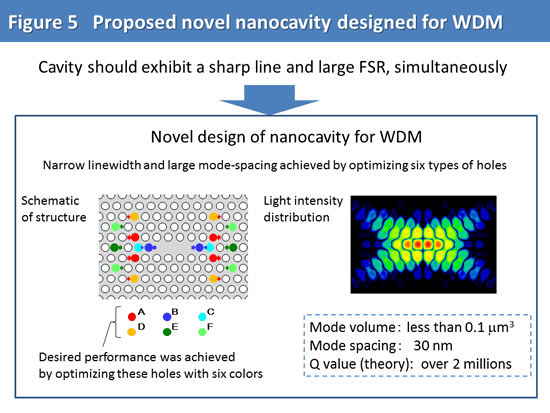
- Novel optical nanocavity design for WDM integration (Figure 5)
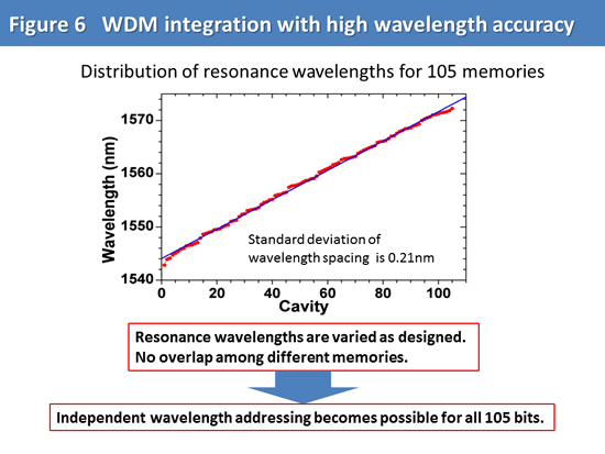
In order to realize large-scale integration of memories with the WDM scheme shown in Fig. 1(ii), it is essentially important to avoid any overlap among different wavelength channels. This means that an optical cavity which has an isolated single resonant mode with sufficiently narrow resonant linewidth is required, but the previous design of optical nanocavities does not satisfy this. NPC has successfully achieved this requirement by adopting a novel nanocavity design in which six different hole positions in photonic crystals were optimized using three parameters. - High resolution WDM integration technology (Figure 6)
In order to actually write/read different bits independently, the fabrication accuracy of the resonant wavelength for each cavity is also essentially important. NPC fabricated photonic crystal devices using high-resolution electron-beam lithography and dry etching techniques and successfully achieved this requirement. Figure 6 shows that the wavelength of all bits were uniformly varied with a sufficiently small statistical disorder.
We plan to combine the present serial integration scheme based on WDM and the parallel integration scheme based on the spatial division multiplexing to realize a matrix integration which will enable further larger number of bits. It is believed that an optical RAM with approximately a kilo-byte capacity will be sufficient for applying to sophisticated high-speed network processing such as routing. Since the present WDM integration scheme can be applied to optical devices other than memories, we will proceed research and development for various photonic processing and transportation with the WDM functionality and integrated them in a single chip.
In addition to that, we believe that the present method can be introduced even in a microprocessor chip used in various instruments for ICT. In fact, advanced microprocessor chips employ the many-core architecture, and it is predicted that on-chip communications among a large number of cores will dominate the power consumption of a chip. Since the present technology will enable ultrafast optical network processing integrated in a small chip, we believe that one can reduce the power consumption of a chip dramatically by introducing on-chip optical network processing in a chip.
Publication
"Large-scale integration of wavelength-addressable all-optical memories on a photonic crystal chip"
E. Kuramochi, K. Nozaki, A. Shinya, K. Takeda, T. Sato, S. Matsuo, H. Taniyama, H. Sumikura and M. Notomi
Nature Photonics (2014).
Glossary
*1 ... Photonic crystal
An artificial structure whose refractive index in periodically modulated by a length scale comparable to the wavelength of light, usually fabricated by semiconductor lithography technology. Since photonic crystals behave as optical insulators, which do not exist in nature, extraordinarily strong light confinement becomes possible and they are therefore expected to realize ultrasmall photonic devices and circuits.
*2 ... Optical nanocavity
An optical cavity is an element which confines light with a certain resonance. Since it is fundamentally difficult to confine light in a small space, miniaturization of high-performance cavities has been difficult. Historically, small cavities whose size is about 10 to 100 times of the wavelength of light have been called “microcavities”. Recently, ultrasmall cavities whose size is comparable to the wavelength of light (the volume is less than 1 µm3) is called “nanocavities”. Various high-performance nanocavities have been realized by employing photonic crystals.
*3 ... Random Access Memory (RAM)
A memory which stores binary bit information and can write/read arbitrary bits with arbitrary timing and order. RAM is widely used in various information processing instruments such as computers, and is normally composed of integrated semiconductor electronic devices including transistors.
*4 ... Wavelength Division Multiplexing (WDM)
Wavelength division multiplexing (WDM) is one of the ways to multiplex the data in which different information is coded in different wavelength. WDM is one of the most important advantages of optical information processing against its electric counterpart. WDM is already employed in today’s optical fiber communication, and it enables us to greatly expand the capacity of communications.


