


Semiconductor quantum dots with single-atom precision
- Electron confinement to nanostructures of atomic building blocks with exact fidelity -
NTT Basic Research Laboratories(NTT-BRL), the Paul-Drude-Institute (PDI; Germany), and the Naval Research Laboratory (NRL: USA) have cooperatively developed a novel quantum dot*1 (artificial atom*2) and combined artificial molecules*2 with single-atom precision of the position and configuration. This has been realized at a clean surface of semiconductor single crystal thin film manufactured by Molecular Beam Epitaxy (MBE)*3 by using low-temperature Scanning Tunneling Microscope (STM)*4 to integrate atoms one-by-one with an atom manipulation*5 technique.
This technology enables us to implement quantum dots with identical properties like natural atoms flexibly at the semiconductor substrate. Usage of these quantum dots enables us to manufacture ultimate quantum devices with atomic-level reproducibility like a single photon source*6 with a uniform wavelength and an array of quantum bits*7 with uniform functions, which have not been available due to statistical errors of structural fluctuations. Furthermore, integration and control of these precise nanostructures*8 will help us to develop a quantum computer and a next-generation technology called 'Beyond CMOS'*9 to overcome the limits of conventional silicon technology.
These results will be published in the UK science journal "Nature Nanotechnology" on 29th, June 2014.
=> Press Release
=> Quantum Solid State Physics Research Group
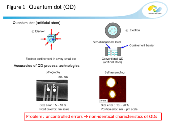
Through the design and processing of materials at the nanometer-level (1 nm = 1/1000000000 m), nanotechnology allows us to create new properties and functionalities not currently available due to the nature of original materials. A quantum dot (QD) is a nanostructure that confines electrons in a nanometer-level narrow space to make quantum mechanical effects evident. Therefore, QD is called an 'artificial atom' and is expected to be applied to a wide range of applications in various fields like optical and electronic devices, display panels, biotechnology, solar cells, and quantum information processing. However, the influence of microfabrication error becomes more serious as the manufactured device becomes smaller. Conventional lithography and self-assembling methods are problematic in the processing precision. Position and configuration of the fabricated nanostructures have included unavoidable variations (Figure 1). Thus, how to improve the device processing accuracy has been a problem to be solved.
If the fabrication and characterization of quantum structures with atomic precision become available at the semiconductor substrate surface, this will be a major leap toward the realization of a new integrated circuit technology expected about 10 years from now by the fusion of 'wafer-level semiconductor technology' and 'atomic and molecular electronics'*10. NTT Basic Research Laboratories (NTT-BRL) has studied quantized states of semiconductor nanocrystals and adatoms by using high quality semiconductor thin film growth technology and low-temperature STM observation. Furthermore, NTT-BRL and PDI have cooperatively cultivated the atom manipulation technology at semiconductor surfaces using the low-temperature STM as a new approach to surpass conventional nanostructure fabrication technologies.
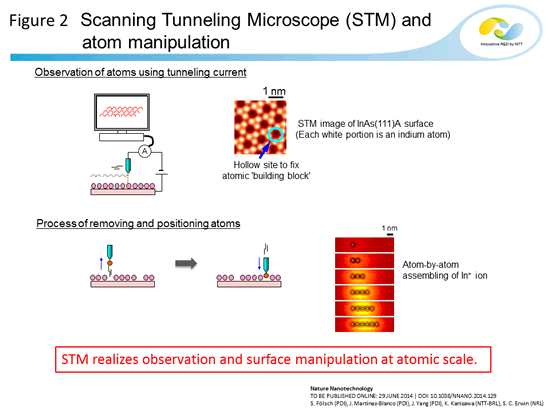
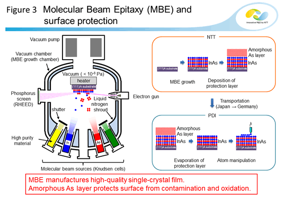
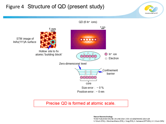
A team of physicists from NTT-BRL, PDI, and NRL has succeeded in building QDs (artificial atoms) and combined nanostructures (artificial molecules) with ultimate atomic-level accuracy of positions and sizes for the first time, which is extremely more precise than any other conventional structure processing methods. We applied an atom manipulation method (Figure 2) using low-temperature STM at a clean surface of a high-quality semiconductor thin film grown by MBE (Figure 3). By the synergistic effect of coupling between extremely high processing accuracy at no difference in single atom and high crystallinity of the semiconductor thin film, we have succeeded in fabricating QDs with identical properties (Figure 4). Moreover, we have succeeded in integrating three QDs of a few nm in a 10 nm square area, meaning that we have achieved ultimate-high-density integration of functional quantum structures. This degree of integration is local but is about 1000 times as high as that of LSIs used in the present computers.
Details of measurements and observation
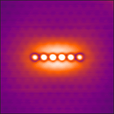
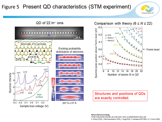
- Precise QDs are exactly composed of a row of ions. Quantized states in these QDs are confirmed to be a result of confinement of electronic states on the semiconductor side. (Figure 4 and Figure 5)
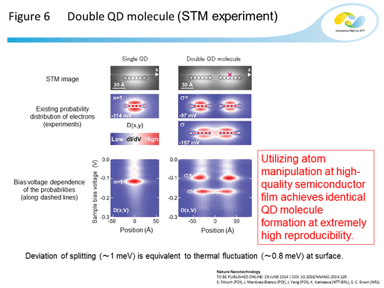
- An artificial molecule composed of two precise QDs (core of six ions for each) shows bonding and antibonding states. The measurement error of the energy level splitting of several artificial molecules is confirmed to be equivalent to thermal fluctuation of the measurement environment. (Figure 6)
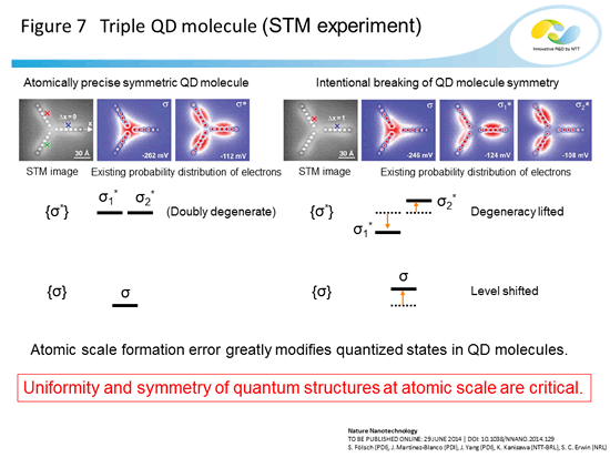
- An artificial molecule is composed of three precise QDs (core of six ions for each). It is experimentally confirmed that atomic-level structural variation significantly influences the quantized states of a very small semiconductor quantum structure, the feature of which is predicted by the theoretical calculation. (Figure 7)
Technical Features
- Use of (111)A surface at single crystal semiconductor thin film
For the base of the atom manipulation, we used an (111)A-oriented surface of indium arsenide (InAs)*11 crystal. The (111)A surface has periodic hollow sites caused by a specific atomic structure of compound semiconductors. The structure formation can be exactly controlled by placing each atom at each hollow site. The high quality InAs thin film has been grown at NTT-BRL on the (111)A-oriented substrate with atomically controlled thickness. After the grown InAs surface was covered by a protection film (amorphous As), the sample was transferred from NTT to PDI. - Atom-by-atom quantum structure fabrication
When the sample was loaded into STM instruments at PDI, the protection film was removed in an ultra-high-vacuum to recover the clean (111)A surface, on which it is feasible to perform atom manipulation. The indium (In) atom is self-ionized at the InAs surface to be +1 charged ion with releasing an electron. By using the low-temperature STM, we can not only observe surface atomic arrangement but also form nanostructures by atom manipulation of these ions as building blocks. Artificial atoms (6 ≤ the number of atoms ≤ 25) have been manufactured by arranging each In atom one-by-one in a line at the (111)A surface. The row of such ions behaves as a 'core' of an artificial atom and electronic states at the semiconductor surface are confined to the induced local potential well. - Analysis and design of artificial atoms and molecules by theory
Density Functional Theory (DFT)*12 at NRL has played a vital role in the analysis and design of artificial atoms and molecules. By the calculation, the states of the artificial atom are found to originate in the quantized electronic states at semiconductor surface, but not atomic orbitals of In adatoms. Moreover, comparison of quantized states among artificial molecules and theoretical results has confirmed that the properties of these nanostructures have atomic-level fidelity without error of structural fluctuation.
We expect that the present achievements will open the door to developing new electronic technology by combining atomic and molecular electronics with semiconductor thin film technology. By exploring novel properties of many integrated atoms and the interaction with semiconductor heterostructures, we plan to develop architectures for quantum computers and high-performance semiconductor devices composed of well-defined semiconductor nanostructures with robust fidelity. Further study will bring many benefits to a broad range of science and technology fields.
Publication information
S. Fölsch, J. Martínez-Blanco, J. Yang, K. Kanisawa and S. C. Erwin
"Quantum dots with single-atom precision"
Nature Nanotechnology (2014).
Glossary
*1 ... Quantum dot (QD)
A quantum dot, or quantum box, is a microscopic structure that confines an electron inside with length, width, and height scales all equal to or smaller than the de Broglie wavelength of free electrons (1 ~ 100 nm). Because the confined electrons obey quantum mechanical statistics, this quantum structure has attracted attention as a key element to develop a quantum computer.
*2 ... Artificial atom and artificial molecule
An artificial atom is a microscopic structure manufactured to reproduce intrinsic properties of natural atoms like the electronic shell structure and Hunt’s rules. A semiconductor quantum dot behaves as an artificial atom. An artificial molecule is a microscopic structure made of artificial atoms that shows properties similar to those of a natural molecule.
*3 ... Molecular Beam Epitaxy (MBE)
Epitaxy refers to a single crystal growth with one particular crystallographic orientation on a substrate. MBE is a vapor growth method, which performs the epitaxy with irradiating beams of atomic or molecular gases of high purity materials to the substrate under an ultra-high vacuum of 10-8 Pa or less. The MBE can control thickness of grown film at atomic layer precision. The single crystal film growth by MBE is an essential technology in the semiconductor field.
*4 ... Scanning Tunneling Microscope (STM)
STM is an electron microscope that scans an atomically sharpened conductive needle (tip) above the conductive material surface as a probe of tunneling current by applying the voltage difference between the tip and the surface at a distance 1 nm or less. By signal processing of the measured tunneling current, STM visualizes local electronic states to observe surface atoms. The STM is also feasible as a tool for atom manipulation.
*5 ... Atom manipulation
Atom manipulation is a surface modification method to detach, displace, and attach atoms flexibly one-by-one by utilizing an atomically sharp needle. This method produces novel nanostructures of integrated atoms at atomic precision, which are available neither in nature nor by chemical reaction. This is one of the most important methods in nanoscience and nanotechnology.
*6 ... Single photon source
Electromagnetic waves including light belong to quanta that show wave-particle duality. When we focus on the particle nature, the minimum unit is called a photon. A single photon source can control the emission of the electromagnetic waves with the accuracy of a single photon. It is an optical element vital to high performances of communication and information processing.
*7 ... Quantum bit
A 'bit' is the minimum unit of information used in computers. Conventional computers perform calculations by using an array of classical bits, which take either '0' or '1' individually. A quantum bit is a unit element in the heart of a quantum computer. With the feature of 'superposition' of the quantum state, the quantum bit is manufactured to take any state (pure state) with the probabilities of '0' and '1' to be p and q (p + q = 1), respectively. Introducing an interaction called 'entanglement' to an array of the quantum bits is expected to realize a quantum computer, which achieves extremely higher information processing speed.
*8 ... Nanostructure
A nanostructure is a microscopic structure formed or processed to have an exact size shorter than 100 nm in length, width, or height. In a wide sense, an object that includes a microscopic structure fabricated with former geometric specifications is referred to as the nanostructure. Since the nanostructure shows unpredictable characteristics from elemental composition of the material due to the microscopic size, it is expected to be usefully applied to future technologies in various fields.
*9 ... Beyond CMOS
The conventional concept of semiconductor device technology (CMOS technology), which is to develop integrated circuits by the scaling trend in accordance with Moore’s law, is forecast to reach the miniaturization limit in the near future due to the possible minimum size. One novel concept is referred to as ‘beyond CMOS’, which aims to overcome this limit by utilizing materials other than silicon and new principles of device operations.
*10 ... Fusion of 'wafer-level semiconductor technology' and 'atomic and molecular electronics'
Prospective views of science and technology of nanostructures are presented as academic and technological roadmaps by several societies and organizations. According to these roadmaps, new technology of integrated circuits is expected to be realized about 10 years from now (around 2025) by combining the atomic-level microstructure technology with the conventional semiconductor production technology.
*11 ... Indium arsenide (InAs)
InAs is a compound semiconductor of indium (In) and arsenic (As). It takes the zinc-blende crystal structure with the direct band gap width of 0.42 eV at cryogenic temperature. It is one of important materials in high-speed electronic and infrared photonic devices. The surface tends to have an electron accumulation layer, which leads to high electric conductivity even at cryogenic temperature.
*12 ... Density Functional Theory (DFT)
DFT is a theoretical calculation method to study many-body system of atoms and molecules. To find mechanically equilibrated states (the total energy minimum situation) of the system, numerical calculations are performed on supercomputers. By using the results, the electronic energy band structures of crystals and surfaces and the stable adsorptive sites of atoms are precisely estimated. DFT is an important method to understand properties of materials as well as predict novel properties of matters by numerical simulations.


