


Nano-profiling of frozen electrons in a semiconductor device
- Probing the microscopic structure of electron solids using magnetic resonance -
A research team comprising members from NTT Basic Research Laboratories(NTT-BRL) and the Japan Science and Technology Agency (JST) has succeeded in observing the crystallization of electrons in a semiconductor device under conditions of low temperature and high magnetic field using nuclear magnetic resonance (NMR)*1. The research team exploits the fact that the effective magnetic field*2 electron spins*3 exert on nuclear spins*4 spatially varies when the electrons form a crystal lattice and the measurement was achieved by using a pristine semiconductor heterostructure*5 and highly sensitive resistively detected NMR.
While it is established that such an electronic state, predicted 80 years ago and known as the "Wigner crystal", exists from the resonance absorption of electromagnetic waves, this is the first time that its microscopic structure has been revealed. The outcome of this study shows that NMR is a powerful means for probing not only the spin but also the charge or orbital state of electrons in a semiconductor, which may lead to elucidation of other exotic phases or the development of materials with novel physical properties. Furthermore, it enables us to quantify the variation of electron density on a nanometer scale induced by randomly distributed impurities. This will be a useful technique for characterizing nanometer-scale electronic devices.
These results will be published in the UK science journal "Nature Physics" on 20th, July 2014.
=> Press Release
=> Quantum Solid State Physics Research Group
A goal of physical science is to elucidate the diverse behaviors of materials at the microscopic level and apply them to develop materials with new physical properties. To this end, it is essential to understand the behavior of electrons in matter at the microscopic level.
Metals and semiconductors are good conductors of electricity, as they host many electrons that can move freely in response to an externally applied electric field. Such an electron, often referred to as a "free electron", travels freely inside the media as if in a vacuum, just as though it were free from the influence of the atoms that constitute the metal or semiconductor or from that of other electrons. A group of such electrons, which behaves like a molecular gas, is called a "free electron gas".
When the interaction between electrons is strong, they can still move while being correlated with each other, like molecules in a liquid. Such a state is often called “an electron liquid” and is well known in the field of condensed matter physics.
The possibility of electrons solidifying into a crystal was first predicted in 1934 by Eugene Wigner, a physicist from Hungary. While electrons’ kinetic energy is reduced as they become more extended in space, since they repel each other via the Coulomb force*6, it is more favorable in terms of the interaction energy for them to be spatially localized. Since the ratio of the kinetic energy to interaction energy depends on the electron density, electrons should solidify into a crystal at some point as their density decreases.
This state, known as a "Wigner crystal", has been confirmed to exist at low temperature in a very dilute two-dimensional electron system*7 on the surface of liquid helium or in a two-dimensional electron system in a semiconductor heterostructure subjected to a strong magnetic field. In semiconductors, which contain impurities, the effects of interaction between electrons may be outweighed by the influence of impurities at low electron density, which interferes with the observation of a Wigner crystal. The role of the high magnetic field is to quantize the electrons' kinetic energy and facilitate the crystallization at higher density. As evidence for electron crystallization, experiments thus far have found resonance excitation modes that are unique to a solid*8 in electromagnetic wave absorption spectra. However, another hallmark of a solid, a fixed interelectron distance coupled with a local electron density that varies in space, has not been observed yet. Furthermore, a means to probe the microscopic structure of an electron crystal has been lacking.
A team comprising members from NTT-BRL and JST performed NMR measurements on a pristine gallium arsenide (GaAs)/aluminum gallium arsenide (AlGaAs) heterostructure containing a high-mobility two-dimensional electron system and obtained resonance spectra of arsenic nuclei constituting the GaAs layer that directly indicate the crystallization of electrons at low temperature and high magnetic field.
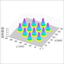
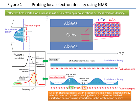
The resonance frequency of nuclear spins is subject to a tiny shift caused by an effective magnetic field exerted by the electrons surrounding the nuclei. From this shift, known as the Knight shift, NMR obtains information about electron spins. In this study, researchers exploited the fact that the Knight shift is proportional to the local electron density at the location of the nuclei to demonstrate the spatial variation of local electron density that results directly from electron crystallization (Figure 1). Furthermore, comparison with computer simulations based on microscopic wave functions of electron solids revealed the microscopic structure of the electron solid.
Details of measurements and observation
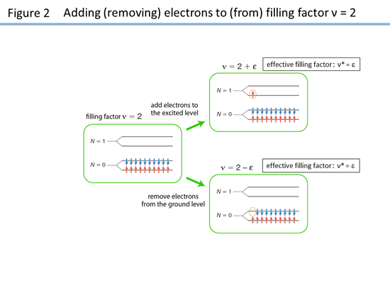
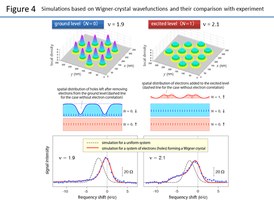
When electrons confined to a two-dimensional plane are subjected to a strong perpendicular magnetic field, their kinetic energies are quantized and the electrons are forced into discrete energy levels. The number of electrons each level can accommodate is determined by the strength of the magnetic field, and the number of filled levels, or "filling factor", ν is an important parameter that dictates the electronic state. For example, ν = 2 means that the spin-up and spin-down branches of the ground level are fully occupied, a situation that can be regarded as an inert background with uniform density and zero total electron spin. Researchers investigated the behavior of electrons added to ν = 2 and holes left after removing electrons from ν = 2 (Figure 2).
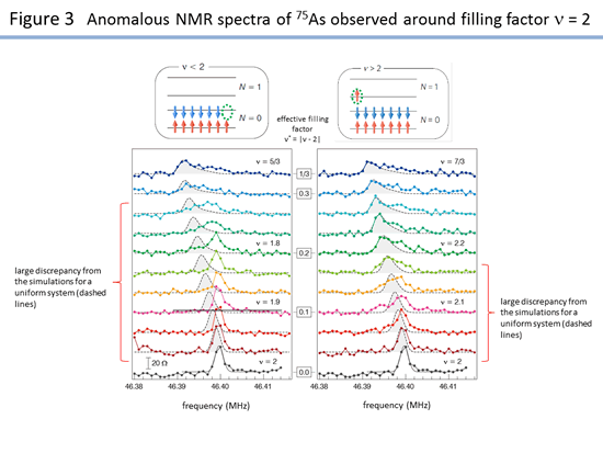
- Resonance spectra of 75As nuclei were measured at various filling factors around ν = 2 at 6.4 tesla and 50 millikelvin*10 (Figure 3). Comparing the observed spectra with simulations assuming a uniform electron system demonstrates that non-uniform states develop at 5/3 < ν < 2 and 2 < ν < 11/5.
- The distribution of local electron density in a Wigner crystal phase is calculated using the ground and excited level wave functions. Simulations based on the calculated density distribution reproduce the spectra measured at ν = 1.9 and 2.1. A detailed comparison of experiment and model calculations reveals the microscopic structure of the electron solids and the effects of electron correlation therein (Figure 4).
Technical Features
- Clean two-dimensional electron system allowing for the formation of a Wigner crystal
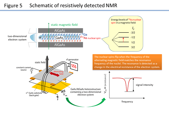
Crystallization of electrons arises from the inter-electron Coulomb interaction. If the density of residual impurities in the host material is not sufficiently low, electrons would be more susceptible to the impurity potential rather than to the interaction with other electrons. It is therefore desirable to reduce the impurity concentration as much as possible in order to observe a Wigner crystal. The research team used a high-mobility two-dimensional electron system grown at NTT-BRL, which enabled the observation of a Wigner crystal without deleterious effects due to impurities. - Probing the local electron density with resistively detected NMR (Figure 1, Figure 5)
NMR measures a tiny shift in the resonance frequency caused by an effective magnetic field exerted by the electrons surrounding the nuclei. The low signal intensity of conventional NMR makes it difficult to perform NMR on a single-sheet electron system. The research team used a resistively detected NMR technique, which was uniquely developed by the team. In resistively detected NMR, magnetic resonance of nuclear spins is detected as a change in the electrical resistance of the electron system, thereby making it possible to selectively and sensitively detect signals from the nuclei in contact with the electron system of interest and to eliminate unwanted signals from the far more abundant nuclei in the substrate and other layers of the heterostructure. This enabled us to clearly observe the anomalous NMR lineshape signifying the spatially varying local density of crystallized electrons.
The outcome of this study shows that NMR is a powerful means for probing not only the spin but also the charge or orbital state of electrons in a semiconductor. In particular, it offers a significant advantage of spatial resolution provided by nuclear spins, allowing one to obtain microscopic information about the electronic state on a nanometer scale. This opens the way to studies of other exotic phases with nontrivial spatial spin/charge order. It also enables us to quantify the spatial inhomogeneity of electron density induced by randomly distributed impurities. This will be a useful technique for characterizing electronic devices facing nanometer-scale miniaturization, where eliminating device-to-device variability is a critical issue.
Publication information
L. Tiemann, T. D. Rhone, N. Shibata and K. Muraki
"NMR profiling of quantum electron solids in high magnetic fields"
Nature Physics (2014).
These experiments were performed through joint research between NTT and JST as part of the Exploratory Research for Advanced Technology (ERATO) "Hirayama Nuclear Spin Electronics Project". The theoretical model and interpretation of data in this work were obtained through discussion with Associate Professor Naokazu Shibata of Tohoku University.
Glossary
*1 ... Nuclear magnetic resonance (NMR)
A physical phenomenon in which atomic nuclei in a magnetic field absorb electromagnetic radiation at a resonance frequency specific to the nuclide. Since the resonance frequency is sensitive to the nature of chemical bonds and the distribution of surrounding electrons, it is used for spectroscopic analysis and physics research.
*2 ... Effective magnetic field
When quantum mechanical particles interact with each other through an interaction that depends on the spin of the particles, it is useful to regard the resulting effect as arising from a virtual, or effective, magnetic field. Electron spins and nuclear spins are coupled via the hyperfine interaction, which in NMR can be regarded as an effective magnetic field exerted by electrons on the nuclei.
*3 ... Electron spin
The quantum mechanical description of an electron comprises variables that specify its internal degree of freedom in addition to a spatial coordinate. This internal degree of freedom is referred to as “spin”, by analogy to the spinning of a classical object. An electron’s angular momentum comprises the orbital angular momentum (associated with its spatial motion) and the spin angular momentum (associated with its internal degree of freedom). Spin is the origin of the magnetic moment of an electron, and the magnetic force of a ferromagnet stems from electron spins aligned in a particular direction. A magnetic field splits the energy level of an electron into two, with the precession axis of the spin oriented along or opposite to the field direction (up spin and down spin, respectively).
*4 ... Nuclear spin
The total of angular momenta possessed by protons and neutrons constituting an atomic nucleus is called a nuclear spin. Nuclear spin is the origin of the very small magnetic moment of atomic nuclei, and each nuclide has its characteristic value. NMR exploits transitions between energy levels of nuclei split by a magnetic field.
*5 ... Semiconductor heterostructure
A layered crystalline structure comprising a junction of heterogenous semiconductor materials such as GaAs and AlGaAs. With each semiconductor material having its characteristic energy band structure, a junction made of different materials allows us to obtain physical properties that cannot be achieved by the constituent materials themselves or their alloys. Semiconductor heterostructures are used in semiconductor lasers and high-electron-mobility transistors.
*6 ... Coulomb force
The force exerted between electrically charged particles. If the charges are of the same sign, then the force is repulsive; if they are of opposite signs, the force is attractive. The strength of the force is inversely proportional to the square of the distance between the particles.
*7 ... Two-dimensional electron system
Semiconductor heterostructures such as GaAs/AlGaAs can confine electrons to a thin region a few nanometers to several tens of nanometers thick owing to its band gap difference. Because the motion of the electrons is restricted to the two-dimensional plane along the heterointerface, such a system is called a two-dimensional electron system. Other examples include those at a Si/SiO2 interface, in single-atomic-layer materials such as graphene, and on a liquid helium surface.
*8 ... Excitation mode unique to a solid
One feature that distinguishes solids from liquids is that both longitudinal and transverse (or shear) waves propagate in the former, whereas only longitudinal waves propagate in the latter. The property that allows a media to transmit transverse waves is elastic resistance to a shear stress (i.e., a stress that arises from the force vector component parallel to a cross section), as characterized by the shear modulus, and this is precisely a defining feature of a solid. In a two-dimensional electron system in high magnetic fields, resonance excitation modes corresponding to oscillations of a Wigner-crystal domain within a pinning potential are observed. For a two-dimensional electron system on a liquid helium surface, a coupled mode of collective oscillation of electrons and capillary waves has been observed as evidence for electron crystallization.
*9 ... Wave function
In the quantum mechanical description of an electron, one cannot determine its position and momentum simultaneously. The state of an electron is specified by a space-time function, known as a wave function, which is obtained by solving the Schrödinger equation. The probability of finding an electron at a point is given by the square of the absolute value of the wave function at that point. The probability distribution of electrons in a semiconductor forming a Wigner crystal at high magnetic field spreads over a finite width around each lattice point, with the microscopic details described by a wave function.
*10 ... Millikelvin
A unit of temperature. One millikelvin is 0.001 Kelvin, and 0℃ corresponds to 273.15 Kelvin.


