


Programmable linear optical circuit realized on a chip
A multifunctional optical device for quantum information experiments using photons
Researchers from Nippon Telegraph and Telephone Corporation (NTT) and the University of Bristol in the UK have developed a multifunctional photonic circuit for quantum information processing and demonstrated its versatility via a series of experiments using single photons.
The photonic waveguide circuit can be re-programmed by configuring electrical signals applied to the module to implement desired circuit configurations. Using planar lightwave circuit (PLC) technology, the reconfigurability is achieved with low-loss and high-accuracy circuit operations. The circuit enables us to significantly reduce the cost and time required for building experimental setups for photonic quantum information experiments and to accelerate research across fundamental sciences and quantum technologies.
This work was published in "Science" on August 13, 2015 (EST).
=> Press Release
=> Quantum Optical State Control Research Group
Background
Among the many candidates for physically realizing qubits for quantum computation and communication, a photon can be used as a stable qubit because it is rarely affected by noise in environment. Furthermore, quantum states encoded in physical degrees of freedom of photons can be precisely controlled with linear optics (such as beam splitters and waveplates). Motivated by these features, photonic quantum information processing (QIP) experiments using linear optics have been under intense study.
Experimental setups for photonic QIP are built on an optical table by precisely arranging many optical elements such as mirrors and splitters. Or, recently, they are fabricated on a photonic chip as a compact and highly stable optical waveguide circuit. However, modifying or re-fabricating such setups sometimes takes a lot of time. Thus, there has been a huge demand for a single reprogrammable optical device that can be used for various QIP experiments.
Achievements
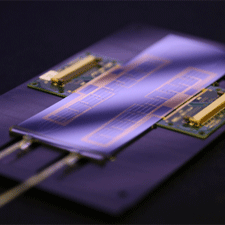
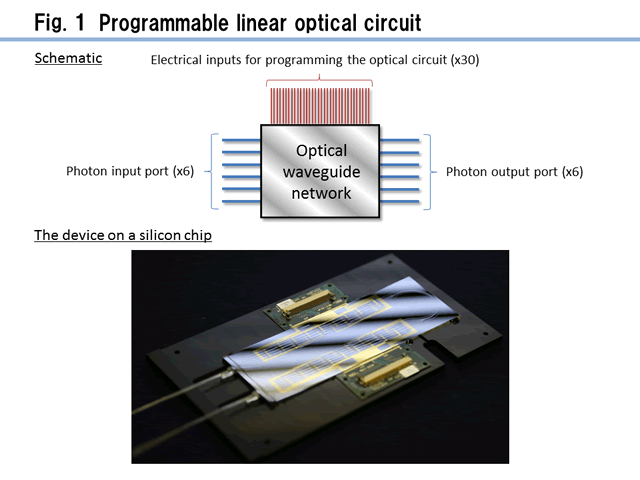
The researchers succeeded in developing the optical device integrated on a photonic chip (Fig. 1) using planar lightwave circuit (PLC) technology. The arrangement of the optical waveguide network in the device can be modified in seconds by configuring electric voltages applied to thin-film heaters arranged across the chip. The researchers further successfully demonstrated the versatility of the device by performing various photonic QIP experiments with single photons. The demonstrations range from implementations of key components for quantum computation (entanglement generations and quantum gate operations) to the performance of state-of-the-art quantum tasks. The total number of circuit configurations used was approximately 1,000.
Technical Features
- Silica-based PLC
Silica-based PLCs are optical circuits that guide light with the same principle as in optical fibers, and they are integrated on a silicon chip by using LSI fabrication technology. Owing to their mass producibility and high stability, PLCs are widely used for current optical communications technologies. In this work, a PLC was designed for its use at the optical wavelength of 800 nm, which is a wavelength suitable for single-photon experiments. The waveguide for the wavelength shorter than that for standard telecommunications (1,550 nm) requires higher fabrication accuracy. Furthermore, the circuit layout of the present device consists of more than 100 nested interferometers – such a circuit configuration has not been required for telecommunications devices. However, mature PLC fabrication technology, the product of years of experience in optical communications technology, has realized the device together with low photon loss and highly accurate operation. - Experimental demonstrations
Quantum optics experiments using single photons are necessary to demonstrate the chip’s versatility. The collaboration with the team at the University of Bristol, a pioneering group in integrated quantum photonics research, was the crucial factor in the success of the project. The series of experiments in this work was readily performed with mature technologies for efficiently generating a bunch of single photons and analyzing the non-classical correlation of the photons output from the chip.
Summary
The researchers have accomplished a longstanding goal of a device for linear-optics based QIP experiments. This achievement will accelerate researches across fundamental sciences and quantum technologies.
Publication information
J. Carolan, C. Harrold, C. Sparrow, E. Martín-López, N. J. Russell, J. W. Silverstone, P. J. Shadbolt, N. Matsuda, M. Oguma, M. Itoh, G. D. Marshall, M. G. Thompson, J. C. F. Matthews, T. Hashimoto, J. L. O'Brien, A. Laing
"Universal Linear Optics"
Science (2015).


