


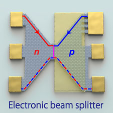
Graphene p-n junction as an electronic beam splitter
- Key component of electron quantum optics using graphene -
NTT Basic Reseach Laboratories (NTT-BRL) and CEA Saclay have demonstrated for the first time that a graphene*1 p-n junction*2 can serve as an electronic beam splitter. The realization of electron beam splitters, key components for interferometry, is a crucial step towards the development of electron quantum optics experiments in graphene
Owing to the probable long coherence length*3 of electrons, graphene is expected to be a useful material for electron quantum optics. In this work, we proposed that graphene p-n junctions can serve as beam splitters and substantiated the performance in large-area graphene grown on silicon carbide (SiC). Utilizing the long coherence length in graphene, it could be possible to make complicated interferometers with multiple beam splitters, which are not able to be fabricated in conventional semiconductors. Experiments using such interferometers will reveal decoherence mechanisms of electrons and enable the generation of quantum entangled electron pairs. These studies contribute to the development of quantum information processing.
This work will be reported in the UK science journal “Nature Communications” on the 4th of September, 2015.
=> Press Release
=> Quantum Solid State Physics Research Group
Background
Quantum optics is a field of research that investigates the wave-particle nature of light based on quantum mechanisms, using interferometers consisting of optical elements, such as mirrors and beam splitters. Knowledge obtained by quantum optics has been applied to quantum cryptography and quantum teleportation. An electron is also a quantum having wave-particle nature like a photon and thus can interfere. A difference between an electron and a photon is whether it is a Fermion*4 or Boson*5. This difference appears in the two-particle interference. Another important difference is the presence/absence of the Coulomb interaction*6. The presence of the Coulomb interaction for electrons has both positive and negative aspects: through the interaction, electron quantum state can be controlled but its coherence is easily destroyed.
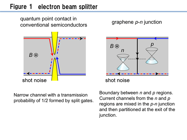
The resultant short coherence length makes electron quantum optics experiments difficult. So far, electron quantum optics has been performed in the quantum Hall state*7, which appears in two-dimensional electron systems under magnetic field, formed in gallium arsenide (GaAs)/aluminum gallium arsenide (AlGaAs) heterostructures*8. In this system, a narrow channel called quantum point contact*9 with the electron transmission probability of 1/2 (Figure 1, left) is used as a beam splitter. A fundamental problem of this system is that the coherence length of approximately 10 µm is as long as the typical size of the interferometer, limiting experiments to the basic level. A way to solve this problem and carry out more advanced experiments is to use graphene, in which the coherence length is expected to be longer. However, since graphene is a gapless material, beam splitters based on quantum point contacts made by depleting local electrons do not work.
Achievements
In this work, a team comprised of members from NTT-BRL and CEA Saclay proposed a new architecture of a beam splitter using a graphene p-n junction. In graphene, electrons injected from the n and p regions are mixed in the p-n junction and then partitioned at the exit of the junction (Figure 1, right). The electron mixing and the subsequent partitioning processes can serve as a beam splitter. The beam splitter behavior has been verified by the measurements of the current noise (shot noise*10).
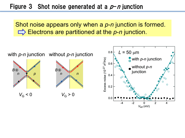
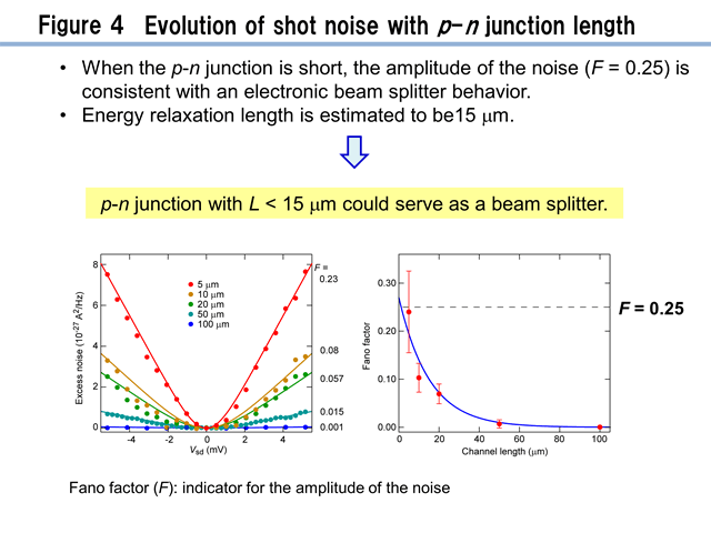
If the p-n junction acts as a beam splitter, electrons are randomly distributed to the n and p current channels, generating the shot noise. We showed that, when the p-n junction is short, the shot noise is generated as expected. As it becomes longer, the noise becomes smaller. Our results indicate that the energy relaxation length, which is an indicator of the loss of the quantum information, is 15 µm and shorter p-n junction can serve as a beam splitter.
Details of measurements and observations
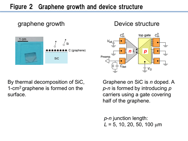
- We used graphene grown on SiC. A p-n junction was made using a top gate covering half of the graphene. The ungated region was n doped, while p carriers were introduced in the gated region. Therefore, a p-n junction was formed at the interface between the gated and ungated regions. We prepared five samples with different p-n junction lengths between 5 and 100 µm (Figure 2).
- All measurements were carried out in a quantum Hall effect regime, which is caused by applying a magnetic field perpendicular to graphene. We measured the shot noise for the system with and without a p-n junction and showed that the shot noise is generated by the p-n junction (Figure 3). This indicates that electron mixing and partitioning indeed occur at the p-n junction.
- Measurements for samples with different p-n junction lengths revealed that the noise decreases with increasing p-n junction length (Figure 4). This result indicates that a p-n junction shorter than the estimated energy relaxation length of 15 µm can serve as a beam splitter.
Technical Features
Graphene growth technique
In general, graphene is obtained by exfoliation from graphite. A drawback of this technique is that the graphene size is limited to several 10 µm. Whereas, the graphene we used were grown by thermal decomposition of SiC substrate. By exploiting the wafer-size graphene, we fabricated devices with different
Future Plans
The architecture of graphene p-n junction is simpler than that of quantum point contact, which is used as a beam splitter in conventional semiconductors, allowing us to integrate several beam splitters within a mesoscopic scale. Utilizing these beam splitters and the long coherence length in graphene, it would be possible to fabricate complicated electronic interferometers, which have not been able to be fabricated. Experiments in these devices would reveal effects of the Coulomb interaction on decoherence. Furthermore, generation of quantum entangled electron pair is expected to be achieved in such devices.
Publication information
N. Kumada, F. D. Parmentier, H. Hibino, D. C. Glattli, and P. Roulleau
"Shot noise generated by graphene p-n junctions in the quantum Hall effect regime"
Nature Communications (2015).
Glossary
*1 ... Graphene
Monolayer of carbon atoms arranged in a hexagonal lattice. Graphene has been attracting much interest both in basic research and applications owing to its unique properties, such as mobility, transparency, flexibility, and chemical stability.
*2 ... p-n juncton
Boundary between n and p regions. In standard semiconductors, a depletion region is formed along the boundary. In graphene, on the other hand, n and p regions adjoin each other without a gap in between because of the absence of the band gap.
*3 ... Coherence length
Distance over which a quantum state can maintain the coherence.
*4 ... Fermion
Fermion is a particle, which follows Fermi-Dirac statistics and therefore the Pauli exclusion principle. Fermions have half-integer spin. Electrons are included in Fermions.
*5 ... Boson
Boson is a particle, which follows Bose–Einstein statistics and therefore multiple bosons can occupy one quantum state. Bosons have integer spin. Photons are included in Bosons.
*6 ... Coulomb interaction
The force exerted between electrically charged particles. If the charges are of the same sign, then the force is repulsive; if they are of opposite signs, the force is attractive. The strength of the force is inversely proportional to the square of the distance between the particles.
*7 ... Quantum Hall state
A phenomenon, which appears in a two-dimensional electron system under a magnetic field. In a quantum Hall state, the Hall resistance is quantized and the longitudinal resistance vanishes. In this state, the current flows only along the edge of the two-dimensional electron system.
*8 ... Semiconductor heterostructure
A layered crystalline structure comprising a junction of heterogenous semiconductor materials such as GaAs and AlGaAs. With each semiconductor material having its characteristic energy band structure, a junction made of different materials allows us to obtain physical properties that cannot be achieved by the constituent materials themselves or their alloys. Semiconductor heterostructures are used in semiconductor lasers and high-electron-mobility transistors.
*9 ... Quantum point contact
Narrow conductive channel connecting two wide conductors. By tuning the width of a quantum point contact, transmission probability of electrons between the conductors can be controlled.
*10 ... Shot noise
Noise originating from particle nature of quanta. An example is the current shot noise originating from the finite charge of electrons.
Note
Complementary results from a group of Osaka University, Kyoto University, and NIMS will be published simultaneously in Nature Communications.


