


Creating a photonic topological insulator by current injection
– A novel principle of controlling topologically robust optical states based on gain and loss –
NTT Basic Research Laboratories and Tokyo Institute of Technology have theoretically found the scheme to create and control an artificial photonic material called “photonic topological insulator,” simply by using optical gain and absorption loss which are electrically tunable. The photonic topological insulator is expected to have applications to on-chip photonic devices that are robust to their structural disorder. This scheme enables to create “topological edge states,” which are peculiar to photonic topological insulators and of disorder immunity, in one-dimensional coupled laser arrays. Moreover, controlling the position and number of such edge states becomes possible. This work will open up a new horizon for engineering photonic topology by the external signal, in addition to the stable performance and novel properties of future topological optical circuits.
This result was published in “Physical Review Letters” on November 20, 2018. The research was partially supported by a JST CREST program (No.JPMJCR15N4), “Study on ultralow-latency optical computing by integrated nanophotonics.”
=> Press Release
=> Photonic Nano-Structure Research Group
Background
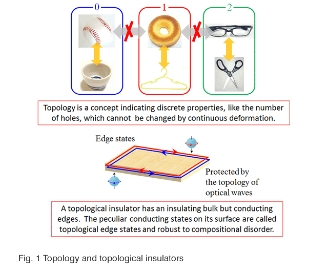
Topology is a mathematic concept considering geometrical shapes of things. It deals primarily with robust and discrete properties, which do not change by continuous deformation such as extension and shrinkage (Fig. 1). The number of holes on things called “genus,” is an excellent example of topological properties. In 2016, the Nobel Prize in physics was shared by Professors David J. Thouless, F. Duncan M. Haldane and J. Michael Kosterlitz, for the achievements of clarifying various topological properties, mainly by introducing the concept to quantum mechanical wave-functions of electrons. The topology of matter waves has led to discoveries of novel physical properties including topological insulators*1.
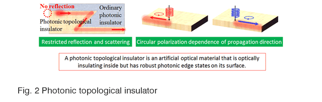
The trend of bringing topology into wave physics has got beyond the limit of electrons and has now extended to photonics, which runs on control of optical waves. Recently, researchers have started to study photonic topological insulators extensively—artificial optical structures, such as photonic crystals*2 , coupled oscillators and waveguides*3 , bestowed with insulation properties and unconventional photonic topology*4 (Fig. 2). A photonic topological insulator does not transmit the light in a particular wavelength region. In the middle of the insulating frequency range, however, it has specific photonic states called topological edge states on its verge. These edge states are robust to structural disorder resulting from the unavoidable incompleteness of device fabrication. Notably, a photonic topological insulator with a two-dimensional structure gives edge states working as guided propagation modes immune from disorder-induced reflection and scattering loss. Moreover, by irradiating the edge with focused laser beams with opposite circular polarizations, two distinct edge states with opposite propagation directions can be individually excited. So, the system can behave like an optical routing device*5.
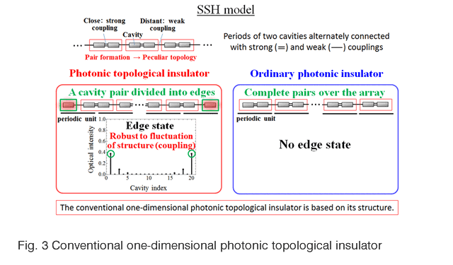
In most previous studies on this new optical material, however, peculiar photonic topology was created by built-in device structures (Fig. 3). Thus, the device topological features, such as the number and position of the edge states, were fixed once fabricated. Moreover, it was considered practically impossible to control freely such properties by an externally applied signal. This limitation would be a drawback to topological optical circuits in their future applications.
Achievements
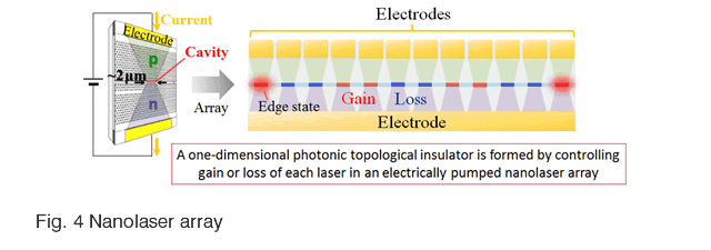
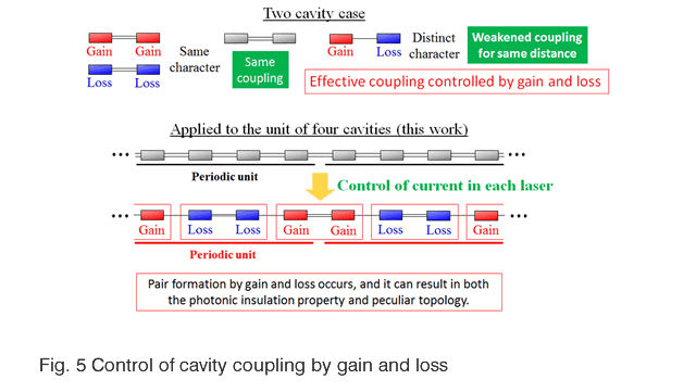
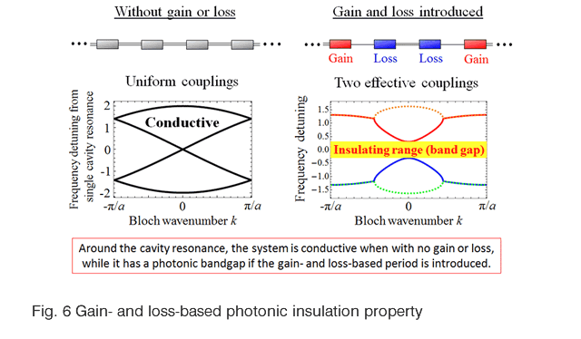
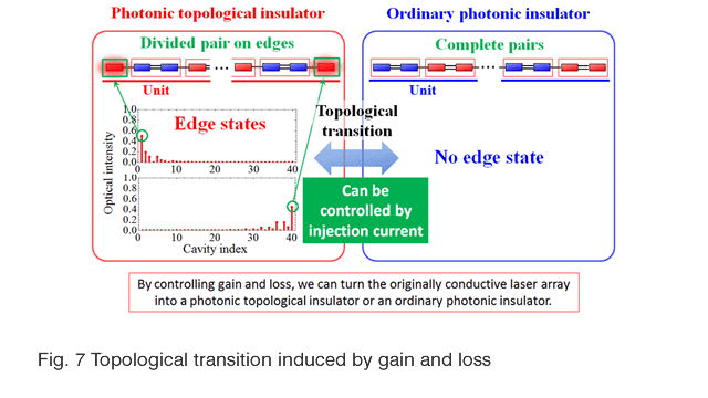
This work demonstrates that NTT has found a way to create and control a one-dimensional photonic topological insulator with only optical gain (amplification) and loss (absorption), which are typically tuned by current injection in commercial lasers, optical amplifiers and modulators, etc. We consider an array of ultra-small laser cavities (nanolasers) that are linearly arranged at equal intervals (Fig. 4). Under no injection current in the device, optical couplings between adjacent cavities are all the same. In this case, it does not have any photonic band gap*6 for the insulation or peculiar photonic topology for the edge states. Here, our scheme adopts a periodic unit of four cavities with current injection, so that two successive cavities with loss and the other two with gain can alternately be aligned inside the array (Fig. 5). We have theoretically clarified that this configuration can produce both a photonic band gap (Fig. 6) and topological edge states (Fig. 7) and confirmed that the system indeed functions as a photonic topological insulator.
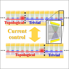
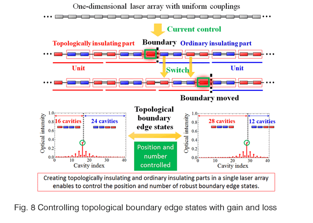
The gain- and loss-based photonic topological insulator also has two edge states that are robust to fluctuations within the structure (cavity couplings) and injection current. Moreover, our scheme enables to create and annihilate both topologically insulating parts with the edge states and ordinary insulating parts without them, of any size, at any position in a single laser array. It means that we can dynamically control the location and number of robust boundary edge states, formed at the boundaries between the topological and ordinary insulating parts, which can be reconfigured by current (Fig. 8). Such flexible topological features could not be obtained in conventional photonic topological insulators. Our technique hence paves the way for new technologies of reconfigurable topological optical circuits, where photonic topology itself could be dynamically controlled in their arbitrary parts.
Principle details
- Conventional one-dimensional photonic topological insulator
For comparison with our scheme, we first describe a conventional one-dimensional photonic topological insulator based on peculiar structural periodicity (Fig. 3). The system considered here is composed of periods of two cavities without any gain or loss. Here, the cavities are alternately connected with a strong coupling (close with each other) and a weak coupling (distant). This makes the system a photonic insulator around the resonant frequency of each cavity.
When we construct an abovementioned array with a limited number of cavities, we have two ways to take its period. One involves the weaker coupling in the middle of the periodic unit, and the other has the stronger coupling there. In the first case, each cavity forming a strongly coupled pair remains separate on each end of the array. Then, we have topological edge states that show localization at these edge cavities, and thereby it is a photonic topological insulator. On the other hand, the second case gives an example of an ordinary photonic insulator without any edge states. Because these two cases differ in structure, it is difficult to alter the presence or absence of the edge states (topology) in such a system.
- Realizing a photonic topological insulator by gain and loss-based coupling control in a four-cavity periodic unit
Here, we explain our scheme. First, we consider two coupled laser cavities (Fig. 5). When the two cavities have gain (or loss) with the same magnitude, their coupling is the same as the case without gain or loss. However, the coupling between a cavity with gain and that with loss becomes effectively weaker.
With this insight, we have found that the cavity-pair formation is possible only by controlling the gain and loss with current, in an equidistant cavity array that is originally of uniform couplings. Here, we introduce a four-cavity periodic unit, where two sequential cavities have loss and the other two exhibit gain. The abovementioned change in the effective coupling then results in the paring of the successive cavities with gain and those with loss. Thus, a photonic band gap is induced in the system (Fig. 6), and choosing a proper permutation in the unit, we have rigorously clarified that the system functions as a photonic topological insulator.
- Creation of edge states and topological phase transition
There are also two kinds of ways to determine the permutation unit in the case of our laser array with the four-cavity periodicity. The first one is of a [gain, loss, loss, gain] like structure, where each cavity of a pair is placed apart at each edge of the array. In contrast, the second is of a [loss, loss, gain, gain] like structure, where the pairs are completed inside the unit and hence the entire array including the edges. In this work, we have theoretically demonstrated that arranging the first type of units makes the system function as a photonic topological insulator with a pair of edge states robust to the fluctuation of the couplings, gain and loss. Meanwhile, the second unit leads to an ordinary photonic insulator. A distinctive feature is that the photonic insulation property and topology here are all created by the gain and loss. Thus, we can induce this change in the presence or absence of the edge states (topological transition) by controlling the injection current.
- Controllable topological boundary edge states
If our technique is applied to an array of many coupled and electrically controlled lasers, one part of the array can be turned into a photonic topological insulator, and the other portion can be made an ordinary photonic insulator. Here, one of the edge states of the topologically insulating part emerges as a robust state localizing at the cavity on the boundary (interface) between the topological and ordinary insulator segments (Fig. 8). This state is called a topological boundary edge state so that it can distinguish from a normal edge state appearing at a physical end of the array.
When the array has a single topologically insulating part and an ordinary insulating part, we can move the boundary edge state by rewriting their sizes via current. In the same manner, arranging many topological and ordinary insulating segments alternately enables to generate as many topological boundary states as the number of the boundaries, with their position being controlled.
Outlook
Recently, the increasing energy consumption and heat generation of information and communications technology (ICT) equipment have been being problematic. This is because high-rate data generation and processing by electronic processors are becoming more and more energy-consuming. A potential proposal for resolving this social issue is to integrate miniature optical network circuits into the processor chip with ultra-small and ultralow-power photonic devices so that it can help efficiently with signal transmission and operation. To this aim, NTT Nanophotonics Center studies semiconductor photonic devices with their sizes comparable to the wavelength of light. Meanwhile, optical integrated circuits are generally vulnerable for reflection and scattering due to structural disorder or mismatch among devices.
Our scheme will contribute to future applications of photonic topological devices that are robust to fluctuation of their structures and external signal. For example, a one-dimensional nanolaser array will achieve stable single-mode lasing and dynamical control of its emission pattern. If the scope of our technique can be extended to two-dimensional arrays, robust optical circuit technologies, such as electrically reconfigurable matrix switches, delay lines and amplifiers, would be established. NTT Nanophotonic Center has a fabrication technique of electrically pumped photonic crystal nanolasers. We are going to fabricate arrays of such tiny lasers for experimental demonstration of our scheme.
Publication information
Kenta Takata and Masaya Notomi
“Photonic Topological Insulating Phase Induced Solely by Gain and Loss”
Physical Review Letters 121, 213902 (2018) [Editors’ Suggestion].
Glossary
*1 ... Topological insulators
A topological insulator is an electronic material that has recently been proposed and discovered. While its inside is insulating, its surface is conducting. This feature stems from the fact that electronic wavefunctions in its periodical atomic structure have peculiar “phase twists” (called Berry phase or geometric phase), which are of topological features. An artificial optical material analogous to the topological insulator is called a photonic topological insulator. This behaves as a photonic insulator inside, but the light can propagate on its edges. The particular conducting states on the electronic and photonic topological insulators are called topological edge states. Note, however, that the edge states of a one-dimensional photonic topological insulator localize at both ends of the linear structure.
*2 ... Photonic crystals
A photonic crystal is a structure of the refractive index that is spatially modulated with a period comparable with the wavelength of light. In most cases, an artificial periodic structure with a pitch of several hundreds of nanometers is formed on a semiconductor material such as silicon and indium phosphide by nanofabrication techniques. A part of photonic crystals works as photonic insulators. Thus, point- and line-shaped defects in such photonic crystals function as minute optical cavities and waveguides because of strong confinement of light to the defects.
*3 ... Coupled cavities and coupled waveguides
An optical cavity is a device to which the light is confined spatially, and an optical waveguide is a device in which the light can propagate. When it is a distance of an order of the resonant wavelength between identical cavities (waveguides), the cavities (waveguides) exchange their optical waves. This is called coupling, and coupled cavities (waveguides) mean cavities (waveguides) that are placed in proximity, so that they can have a significant magnitude of coupling.
*4 ... Photonic topology
Photonic topology indicates the configuration of the abovementioned discrete phase twists of the photonic states that can exist in a certain periodic structure. Here, peculiar photonic topology represents the situation where the photonic topology of the states around an insulating range (photonic band gap) is distinct from the vacuum (air) and other homogeneous media. This is the source of the topological edge states.
*5 ... Optical routing device
In an optical routing device, the destination (output port) of the photonic signal varies depending on a certain degree of freedom of the incident light. Such a device is considered to contribute to electricity saving because it does not use an electric signal for its output control. The optical routing function of the photonic topological insulator is based on the optical spin angular momentum of the edge states, compatible with the circular polarization of the incident optical beam.
*6 ... Photonic band gap
The photonic band structure means the illustration of possible optical frequencies versus each propagation direction of light (Bloch wavevector). A photonic band gap is a blank in this band structure, where light propagation in any direction is prohibited. An optical material hence serves as a photonic insulator for wavelengths within its photonic band gap.


