


Successful nanowire lasing at room temperature in the optical communication wavelength range
— A path to optical-electronic circuit integration for telecom-band micro laser source—
NTT Basic Research Laboratories succeeded in lasing at room temperature in the optical communication wavelength range (not realized by nanowires) by creating a high-quality nanowire*1 laser structure with a thickness of about 1/100 of a human hair. We realized the nanowire structure by using a method to form a semiconductor nanostructure that was developed independently by NTT. We also realized lasing at room temperature in the whole telecom-band range of 1300-1600 nm by precisely modulating the nanowire structure. This technology is expected to produce a seamless connection between direct formation of a coherent light source (which has been the biggest obstacle for optical-electronic integrated circuits*2) and an optical fiber communication network. The result has been published in Science Advances (US science journal) in February 22, 2019 (US: EST 14:00).
Part of this research was made possible by Grant-in-Aid for Scientific Research provided by the Japan Society for the Promotion of Science.
=> Press Release
=> Quantum Optical Physics Research Group
Background
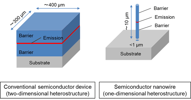
In a semiconductor light-emitting device, a multi-layer structure (two-dimensional heterostructure*3) is employed consisting of an emission layer, which emits the light, and a barrier layer, which confines the injected electrons (Figure 1 - Left). Controlling the thickness of this emission layer and material/composition ratio realizes control of the lasing wavelength or reduction in power consumption, etc. For example, when a light emitting layer is formed with two types of elements (i.e. indium and arsenic), we can control lasing in the whole optical communication wavelength range of 1300–1600 nm by only adjusting the thickness of the emission layer, enabled by the quantum mechanical effect, in principle. In the semiconductor laser source currently used in optical communication, however, an emission layer is used where the composition ratio of four elements (i.e., generally, gallium, indium, arsenic, and phosphorus) is accurately controlled. Using these multiple elements is necessary to prevent a misalignment of interatomic spacing (lattice mismatch*4) occurring between layers with different lattice spacing. If this lattice mismatch is large, dislocations may be formed in the semiconductor crystal, deteriorating the lasing characteristics.
Recently, a one-dimensional nanowire structure with a diameter of 1 μm or less, has received much attention as a method to bypass this lattice mismatch (Figure 1 - Right). Because a nanowire has a very small diameter, it is possible to release the strain caused by the lattice mismatch in the lattice deformation along the radial direction. This allows us to select a multi-layer structure material and a growth substrate that are not restricted by the lattice mismatch. This means we will be able to control lasing wavelength in a wide range of wavelength bands including the optical communication wavelength range (1300–1600 nm) by just changing the thickness of the emission layer consisting of indium and arsenic, irrespective of the growth substrate material.
In recent years, in view of these excellent characteristics, the nanowire is being expected to be applied as a microlaser source (which can be directly formed on a silicon optical-electronic integrated circuit) in the telecom-band wavelength range. The most difficult problem is directly forming the light source in a silicon optical-electronic integrated circuit, where many function elements (e.g., light source, detector, modulator, etc.) need to be integrated in one chip. If we realize nanowire lasers in the telecom-band wavelength range, not only can we directly form the laser source in a silicon optical-electronic integrated circuit but we can also control the formation position with high precision. It is also expected that we will be able to lower the optical loss caused by direct bonding with the optical waveguide. So far, however, nanowire lasing at room temperature has been done only in the short-wavelength range of 300–900 nm and not in the telecom-band range (1300–1600 nm).
Up to now, a method to create nanowire lasers using metal (gold or silver) as a catalyst has become widespread. However, these catalysts are incorporated in the semiconductor during growth. The catalyst material atoms act as impurities, and may deteriorate the lasing characteristics in minuscule structures such as nanowires. In particular, because the optical gain*5 in the emission layer is relatively smaller in the telecom-band wavelength range compared to the short-wavelength range material, the effect of impurities may be serious.
Research results
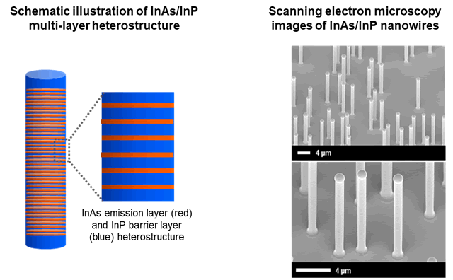
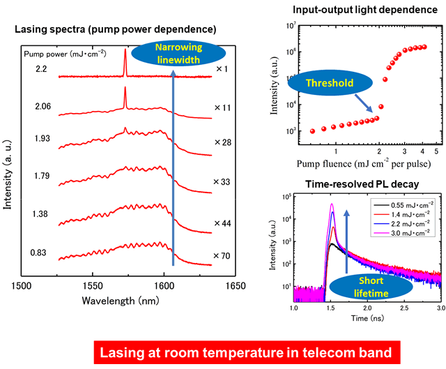
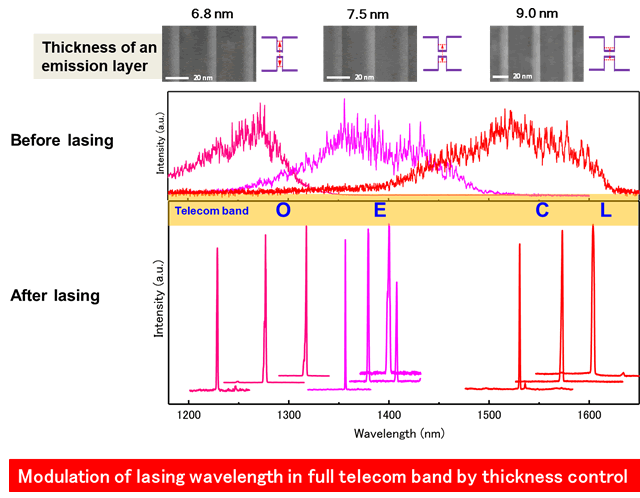
The research team developed a method (See technical point (1).) to grow nanowires using indium metal as the catalyst (indium is one of the element constituting the emission layer/barrier layer structure, and it will not become an impurity) without using conventional different metals (e.g., gold or silver). Using this method, we created a multi-layer nanowire laser structure consisting of a catalyst metal and a single element in each layer (the emission layer contains indium arsenic (InAs) and the barrier layer contains indium phosphorus (InP)) (Figure 2). Normally, this is a combination of layers that cannot be made because the two-dimensional heterostructure has a large lattice mismatch. We examined the lasing characteristics caused by photoexcitation from this structure and successfully observed lasing at room temperature in the vicinity of 1570 nm (telecom-band wavelength range) as a nanowire structure for the first time (Figure 3). We also demonstrated that we can control the lasing wavelength in the 1300–1600 nm range by precisely changing only the thickness of the emission layer (Figure 4). This covers the full range of optical communication wavelength currently being used from O and E to C and L bands.
Future development
Since the nanowire structure is less susceptible to a lattice mismatch, it is possible to create the nanowire structure on a heterogeneous semiconductor substrate. We will expand this method to directly form the microlaser source on silicon substrate. The microlaser source is the biggest challenge for silicon-based optical-electronic integration circuits, i.e. silicon photonics. If we can implement the optical communication wavelength nanowire laser directly on a silicon optical-electronic integration circuit, a seamless connection is possible. This not only dramatically reduces the light loss in the optical interconnection but also avoids the need of the wavelength conversion to adapt to the existing optical fiber system. We will develop a nanowire structure with a single quantum dot that will be a single photon or entangled photon pair generation source; we will also work on developing the nanowire structure as a light source for silicon quantum photonics, which is a quantum light integrated circuit and is becoming an increasingly popular research field.
Technical points
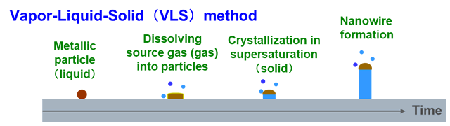
- Self-catalyzed Vapor-Liquid-Solid (VLS) growth method
The semiconductor vapor-phase growth method flows the semiconductor material source (Vapor) into the reactor. If a minute metallic particle (liquid) is present in the reactor, the semiconductor material is dissolved in the catalyst. When the dissolved semiconductor material crystallizes (solid) under supersaturation, a nanowire with a diameter determined by the size of the metal catalyst particle (Figure 5) can be created. This is called the Vapor-Liquid-Solid (VLS) growth method. So far, gold or silver, which form impurities for semiconductors, has been widely used as the metal catalyst; this time, the research team succeeded in using indium metal as the metal catalyst where indium metal is a semiconductor constitutional material. This results in the creation of a nanowire structure that does not have any impurities mixed in and has high material purity. - Nanowire emission layer homogeneity and interface control
Because a nanowire has a very small diameter, it is necessary to place multiple emission layers in one nanowire for lasing. When you want to greatly improve the efficiency of a nanowire and control lasing wavelength, the following factors become critical:
- Homogeneity of the thickness of the emission layer
- Abruptness of each interface of the emission layer/barrier layer
- Inhibition of the disturbance of the crystal
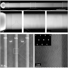
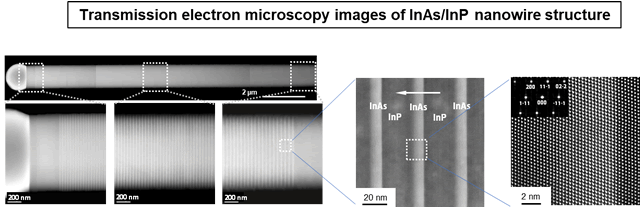
The research team was successful in controlling the thickness homogeneity of multiple emission layers in a nanowire, regardless of the location, by accurately modulating the growth condition (Figure 6). Furthermore, even if we used a combination of semiconductors (i.e., indium arsenic and indium phosphorus) that cannot be grown due to the large lattice mismatch in a two-dimensional heterostructure, we realized a coherent interface between the emission layer and the barrier layer, which is abrupt and undisturbed at the atomic level in a nanowire. - Formation of an optical resonator by a single nanowire
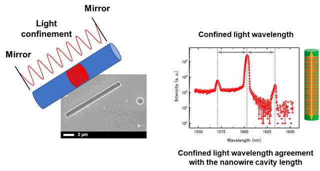
To obtain lasing, an optical resonator structure is needed to confine the light emitted from the emission layer. In a nanowire laser in the conventional telecom-band range, the nanowire itself only functions as the emission layer and a mirror is necessary for the formation of the optical resonator. We have succeeded in making nanowires themselves function as optical resonators (Figure 7). This means that the top and bottom part of the nanowire functions as very flat mirrors, strongly confining the light in the nanowire. This makes it unnecessary to form an optical resonator after nanowire fabrication, greatly simplifying the fabrication process.
Publication information
Guoqiang Zhang, Masato Takiguchi, Kouta Tateno, Takehiko Tawara, Masaya Notomi and Hideki Gotoh
"Telecom-band lasing in single InP/InAs heterostructure nanowires at room temperature"
Science Advances 22 Feb 2019:Vol. 5, no. 2, eaat8896
Terminology
*1 ... Nanowire
A nanowire is a nanostructure in the shape of a wire, having a diameter (several tens through several hundred nanometers) that is 1/100 or less of the thickness of a human hair. Instead of the usual top-down microfabrication method, the bottom-up method is generally used, which directly synthesizes a nanowire on the growth substrate in terms of crystal quality, etc. This method has high degree of structural freedom enabling you to form heterogeneous materials in one nanowire, define a nanowire in any location, and synthesize it on not only semiconductors but also metal or superconductors, etc. Because its nanoscale thickness can develop a quantum-mechanical effect, its application in a wide range of areas has been gaining attention in such areas as photodetection elements, solar cells, biosensors, transistors, etc.
*2 ... Optical-electronic integrated circuit
In a large-scale integrated circuit (LSI IC), in which a large number of electronic components are integrated, the signal transmission speed accompanying the miniaturization of electrical wiring is approaching the limit. As one breakthrough method to overcome this problem, transmitting signals in the form of optical signals, not electrical signals, is expected. An optical integrated circuit can achieve this purpose; optical elements, the basis of the optical waveguide (and electronic components), are integrated in one chip. If you implement an optical integrated circuit on a silicon (Si) substrate, you can use many conventional Si LSI technologies. Silicon photonics are the focus of research by various corporations (e.g., Intel) and universities. However, since Si itself is a material in which light cannot be efficiently produced, the biggest hurdle is to realize a microlaser source among the optical elements to be integrated.
*3 ... Heterostructure
A heterostructure is defined as a structure that bonds individual materials with different compositional elements. Generally, a semiconductor laser consists of an emission layer that emits light and a barrier layer that confines injected electrons in the emission layer; these layers form a heterostructure that bonds different materials in each layer.
*4 ... Lattice mismatch
Atoms constituting a crystal are arrayed in specific interatomic spacing. This defines a lattice constant and if the constituting elements differ, the lattice constant changes. In a heterostructure, usually this lattice constant does not match. This is called a lattice mismatch. When this occurs, there is a large distortion in the crystal structure in each layer of the heterostructure, causing a disturbance in the crystal (crystal defect), etc. As for compound semiconductors, used in lasers, etc., three or more types of elements are precisely formulated to resolve the lattice mismatch, and a heterostructure without a lattice mismatch is used.
*5 ... Optical gain
The difference between optical loss and amplification occurring in the laser is called optical gain. Lasing requires that amplification exceeds the loss. The degree of amplification is based on the optical transition rate of the media (rate to emit the light) and, in the case of semiconductors, the amplification tends to be smaller as the semiconductor shows long-wavelength emission. One of the reasons that lasing in the telecom-band range is more difficult compared to that in visible wavelength is the difficulty to increase the optical gain.


