


Realization of an ultra-energy-saving electro-optic modulator and highly-efficient optical transistor
- Progress towards energy-saving and high-speed opto-electronic signal processing -
NTT Basic Research Laboratories have developed an electro-optic modulator and “optical transistor” with the lowest energy consumption yet reported anywhere in the world.
In general, opto-electronic devices such as electro-optic modulators and photodetectors suffer from high energy consumption primarily due to their high capacitance, and hence it has been difficult to realize a tightly-integrated opto-electronic information processing technique. We have achieved opto-electronic devices with the smallest ever capacitance at the femto-farad level by using a photonic crystal nanostructure. As a result, we have demonstrated an extremely-low-energy electro-optic modulator and an "optical transistor", which transfers a high-speed optical signal to another light with gain. This nanoscale technology will provide new opportunities for a nanophotonic computing platform with extremely low energy consumption and high-speed performance.
This result was published in “Nature Photonics” on April 15, 2019. The research was supported by a JST CREST program (No.JPMJCR15N4), "Study on ultralow-latency optical computing by integrated nanophotonics".
=> Photonic Nano-Structure Research Group
Background
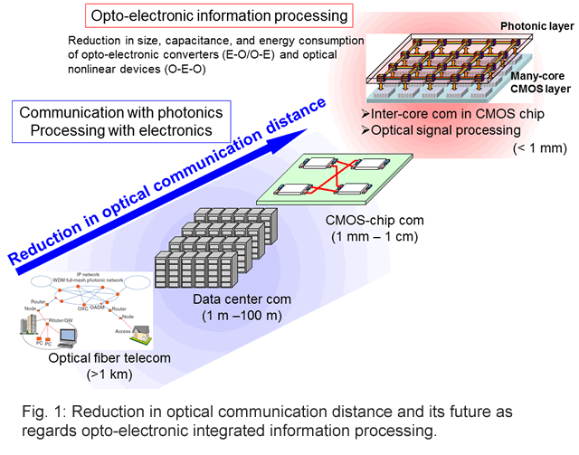
An information processing and computing platform based on complementary metal oxide semiconductor (CMOS) electronics technology*1 has been developed in accordance with Moore’s law*2. However, the potential for progress with integrated electronic circuits is gradually reaching its limit in terms of operating speed and energy consumption due to the physical restrictions of nanoscale fabrication and integration density. Therefore, although photonics technology has been used for long-haul optical communication, there is a demand for photonics to be employed in signal processing and computing components in close conjunction with electronic circuits (Fig. 1).
To this end, we need an electrical-to-optical (E-O) converter that employs an electro-optic modulator (EOM) and an optical-to-electrical (O-E) converter that employs a photodetector (PD) to greatly reduce both size and energy consumption and thus achieve dense integration on a chip. On the other hand, we also need an optical nonlinear device (which can control the optical signal similarly to an electronic transistor) that can outperform existing electronic processors in terms of operating speed. Such optical nonlinear devices have been studied, for example, by combining E-O and O-E converters and configuring an O-E-O converter. However, both the size and energy consumption have been very large, since a strong light is generally needed to reveal the optical nonlinear effect.
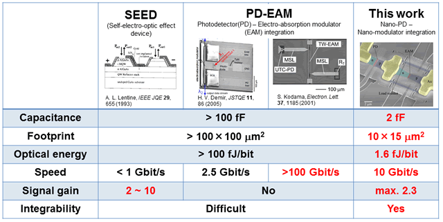
In the photonic research field, opto-electronic devices such as O-E-O converters have been studied for more than two decades for the purpose of computing. However, they were not practical because of their large size, large energy consumption, and slow operating speed of less than 1 GHz. The fundamental problem stems from the capacitance*3, which is as large as 100 femtofarads (fF). This requires a high electric charging energy proportional to the capacitance, and also results in slow operation due to the large RC time constant*4, which is also proportional to the capacitance. To solve these problems, the capacitance of opto-electronic devices and integration has to be greatly reduced. NTT has been developing a semiconductor nanostructure called photonic crystals*5 with which to realize various tiny optical devices. In this work, we used our nanotechnology to demonstrate E-O/O-E/O-E-O devices with extremely small capacitance and energy consumption that cannot be achieved with any other technology.
Achievements
NTT has developed nanoscale photonic crystal technologies and demonstrated an EOM with extremely small capacitance and operating energy, and subsequently realized an optical transistor based on O-E-O integration.
- Electro-optic modulator (EOM) with lowest ever reported energy consumption
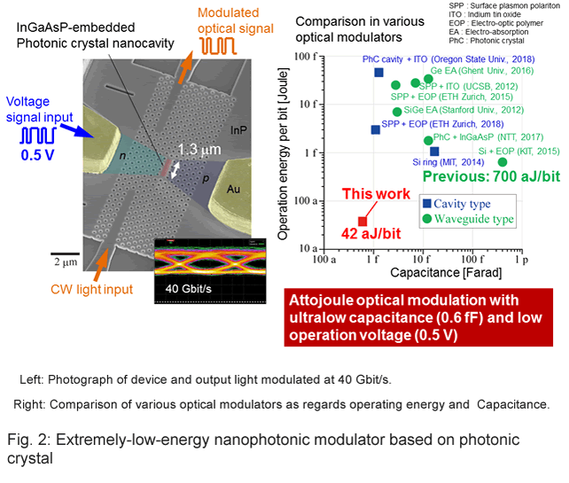
We fabricated a tiny EOM by using a photonic crystal nanocavity*6 (Fig. 2, left). High-speed optical modulation was observed for a voltage signal input with a bit rate of 40 Gbit/s. The operating energy was only 42 attojoules per bit (aJ/bit), which is the lowest value for any optical modulator regardless of material or structure (Fig. 2, right). - Realizing an O-E-O converter with extremely-low integrated capacitance
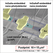
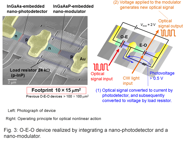
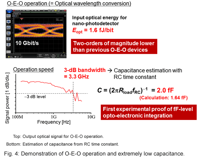
We realized an O-E-O converter by closely integrating the nano-EOM and the nano-PD (Fig. 3, left). In the operation, a high-speed optical signal with a bit rate of 10 Gbit/s is converted to current by the nano-PD, and subsequently converted to voltage by the load resistor. This voltage is applied to the nano-EOM, and thereby the signal is transferred to another light with a different wavelength (Fig. 3, right). This is optical wavelength conversion, which is an optical nonlinear action*7. Our O-E-O converter requires an optical energy of only 1.6 femtojoules per bit (fJ/bit), which is more than two orders of magnitude lower than previously reported O-E-O converters (Fig. 4, top). Our analysis of the operating speed and RC time constant*4 showed that the device capacitance was only 2 fF. This is the first experimental proof of opto-electronic integration with fF capacitance. - Realizing optical transistor*8 action
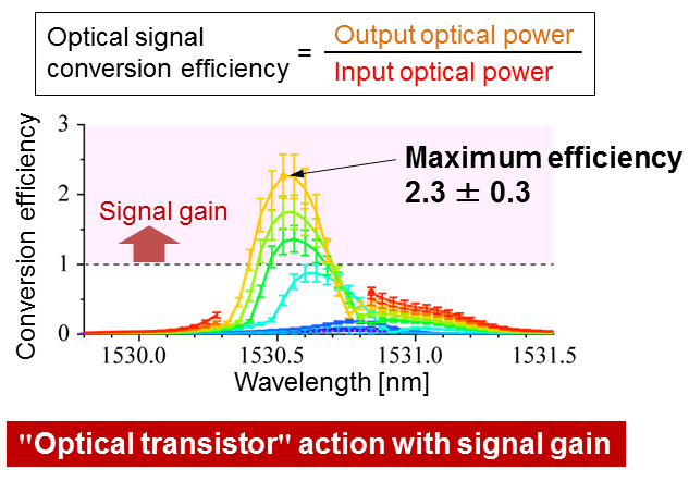
With the optical wavelength converter operation mentioned above, the output signal power can be more than twice than that of the input optical signal (Fig. 5). This reveals the signal gain achieved in the optical nonlinear operation, which is proof of "optical transistor" action. In fact, it has been difficult to reduce the size and energy of previous O-E-O devices (Fig. 6). Thanks to the signal gain, our optical transistor will be able to be cascade-connected and thus realize densely-integrated signal processing in a photonic layer.
Outlook
Our demonstration of the nano-EOM and O-E-O transistor, which have a much smaller size and lower energy consumption than other technologies, will enable us to employ photonics in the novel field of signal processing in contrast to the traditional role of photonics in signal communication. One such application is a photonic network on a chip, in which high-speed optical signals are communicated at high density between many cores in a CMOS chip thus enabling us to realize efficient parallel computing. Furthermore, the optical transistor with signal gain will also be important for realizing high-speed optical processing, which electronics alone cannot achieve. This will lead to the development of novel opto-electronic integrated processors and computers (Fig. 1).
In the near future, we will enter the age of the cyber-physical system (CPS) society in which the real world (physical world) and the cyber world will be intimately connected. In such a society, vast amounts of information from the real world will serve as input requiring an immediate response from the cyber world. Such real-time processing is difficult with existing CMOS technology. Photonic technologies such as those achieved in this work will overcome the current limitations of information processing techniques and contribute to the next-generation CPS society.
Technical points in detail
- An EOM using a photonic crystal nanocavity
To realize an extremely small EOM, we employed a photonic crystal nanocavity fabricated using InP semiconductor material. We employed a point defect with three airholes missing from the photonic crystal, which formed a nanocavity with a length of only 1.3 µm (Fig. 2, left). We embedded an InGaAsP material, which exhibited strong optical nonlinearity, in the nanocavity by using our buried heterostructure technique*9. This nano-fabrication technique is unique and advantageous for our work at NTT. When a voltage signal is applied to the pin junction of the EOM, the Franz-Keldysh effect*10 occurs in the nanocavity and consequently changes the resonant transmission of light. This successfully modulates the light at a high bit rate of 40 Gbit/s. The operating energy for the modulation is dominated by the charging energy used for the capacitance of the EOM. Since our nano-EOM has a capacitance of only 0.6 fF and an operating voltage of only 0.5 V, this energy is suppressed to only 42 aJ/bit (Fig. 2, right). - An O-E-O transistor realized by integrating a nano-PD and a nano-EOM
A photonic crystal nano-PD embedding an InGaAs absorber can be monolithically fabricated with a nano-EOM on the same substrate. The close integration of the nano-PD and nano-EOM results in the successful configuration of an O-E-O converter (Fig. 3). The footprint and capacitance of this integration are still only 10×15 µm2 and 2 fF, respectively. These are both two orders of magnitude smaller than previously reported O-E-O converters. In the experiment, an optical signal with a bit rate of 10 Gbit/s is converted into current by a nano-PD, and subsequently converted to voltage by a load resistor. The nano-EOM is driven by this voltage to modulate another light at a wavelength different from that of the input optical signal. This is the optical wavelength conversion operation. Conventionally, integrated electrical amplifiers are required when converting an optical signal into a signal with a voltage high enough to drive an EOM. However, our device can perform this conversion by using just a high load resistance of 24 kwithout any amplifiers, and therefore greatly suppresses the energy consumption. Thanks to the ultralow capacitance of 2 fF, this high resistance does not significantly degrade the RC time constant. Consequently, this allows a high-speed operation of 10 Gbit/s with an ultralow operating energy of only 1.6 fJ/bit.
Publication information
Kengo Nozaki, Shinji Matsuo, Takuro Fujii, Koji Takeda, Akihiko Shinya, Eiichi Kuramochi, and Masaya Notomi,
"Femto-farad optoelectronic integration demonstrating energy-saving signal conversion and nonlinear functions"
Nature Photonics, vol. 13, pp. 454–459 (2019)
Glossary
- *1 ... CMOS electronics technology
- CMOS is a technology for constructing electronic transistors that is also used in electronic digital logic circuits. The advantages of CMOS, which include a low fabrication cost and low energy consumption, mean that it is widely used in large-scale microprocessors with dense integration. Its miniaturization and dense integration have developed in accordance with Moore’s law. However, this development is gradually approaching its physical limit as regards fabrication and saturation in terms of energy consumption.
- *2 ... Moore’s law
- Moore’s law states that the number of transistors in a densely integrated circuit doubles approximately every 18 – 24 months.
- *3 ... Capacitance
- Capacitance is the ability of an electronic component to store energy in the form of an electrical charge. Opto-electronic devices generally include a metal electrode and a semiconductor pin junction, and hence have a capacitance (C). Since such devices require a driving voltage (V) during operation, the corresponding electrical charge of Q = CV has to be dynamically stored in the device capacitance. Therefore, a reduction in capacitance results in a reduction in the electric energy consumption of the opto-electronic devices.
- *4 ... RC time constant
- An RC time constant is a measure that indicates how long it takes a certain capacitance to charge to a certain voltage level. This time constant is determined by the product of the resistance and the capacitance in the RC circuit.
- *5 ... Photonic crystal
- A photonic crystal is a structure whose refractive index is spatially modulated with a period comparable to the wavelength of light. In most cases, an artificial periodic structure with a pitch of several hundreds of nanometers is formed on a semiconductor material such as silicon or indium phosphide with nanofabrication techniques. Some photonic crystals function as photonic insulators. Thus, point- and line-shaped defects in such photonic crystals function as minute optical cavities and waveguides because of the strong confinement of light in the defects.
- *6 ... Nanocavity
- An optical cavity is an element that confines light at a certain resonant wavelength. Since it is fundamentally difficult to confine light in a tiny space, the miniaturization of optical cavities has been difficult. Historically, small cavities with a size about 10 to 100 times that of the wavelength of light have been called “microcavities”. Recently, ultrasmall cavities called “nanocavities” and whose size is comparable to the wavelength of light (the volume is less than 1 m3) have been formed by employing photonic crystals.
- *7 ... Optical nonlinear action
- When light passes through optical nonlinear materials such as semiconductors, the refractive index and/or the absorption coefficient changes nonlinearly according to the light power level and consequently the output power and/or the phase of light is modulated. If multiple light injection is employed, various optical functionalities such as optical-optical switching and optical wavelength conversion can be performed.
- *8 ... Optical transistor
- "Optical transistors" are not in common use, but here one is used as a device with optical input and output ports that performs an optical nonlinear operation with signal gain. In our work, O-E-O operations are analogous to a three-terminal transistor, when we assume the light input into the PD and EOM to be the gate and source voltages, respectively, and assume the light output from the EOM to be the drain voltage. We expect it to be used as an optical nonlinear device for controlling optical signals in future opto-electronic information processors.
- *9 ... Buried heterostructure technique
- This technique involves heterogeneously embedding semiconductor materials (InGaAsP and InGaAs for EOM and PD, respectively, in our work) in the substrate semiconductor material (InP). This enables us to embed the transparent material and absorptive material in arbitrary positions, and thereby different optical functionalities can be realized on the same substrate. In our work, we use an ultra-compact buried heterostructure to fabricate the photonic crystal nano-EOM and nano-PD.
- *10 ... Franz-Keldysh effect
- The Franz–Keldysh effect is the change in the optical absorption and refractive index in a semiconductor that occurs when an external electric field is applied. This effect originates from the reduction in the bandgap energy and the shift of the optical absorption edge wavelength to the longer side, which changes the power and the phase of the light transmitting through the material. When it occurs in an optical cavity, it appears as a wavelength shift and a change in the peak transmission of the resonance, and consequently modulates the light output.


