


Demonstration of a high performance optical logic gate for ultralow-latency data processing
– One more step towards photoelectronic converged data processing infrastructure –
Nippon Telegraph and Telephone Corporation (NTT, Head office: Chiyoda-ku, Tokyo; President & CEO: Jun Sawada) have demonstrated a high performance optical logic gate for ultralow-latency data processing. Electronic computation circuits are composed by logic gates. However, the increase of latency is getting a more serious problem as well as the high energy consumption problem. Our research group have succeeded in low-loss and high-speed operation of a very small optical logic gate driven by only “light-interference” for the first time in the world. According to the presented device, we can perform ultralow latency and wavelength insensitive Boolean logic operations (“AND”, “XNOR”, “NOR” etc.) with using a single device. By integrating high-speed wavelength-selective optical modulators, it would be possible to assign independent operations for each wavelength channel (so called “wavelength multiplexed parallel operation”). It is expected that it will become one of elemental devices for novel photoelectronic converged processors for ultralow latency pattern matching and vector operations for photonic neural network applications.
A report on this development was published in “Communications Physics” on March 6, 2020. This work was supported by Japan Science and Technology (JST) CREST (JST) CREST (“Study on ultralow-latency optical computing by integrated nanophotonics”, #JPMJCR15N4) .
=> Photonic Nano-Structure Research Group
Background
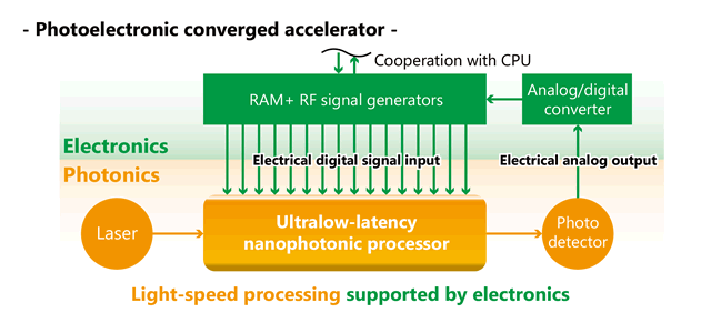
Up to date, data processing infrastructures based on complementary metal oxide semiconductor (CMOS)*1 have continuously grown owing to the huge progress on semiconductor fabrication technologies. However, the miniaturization of the electronic circuits also has brought other issues; the increase of leak current and wiring resistance, which totally stops the continuous growing in the near future. According to this fact, the exploration of novel technologies towards next scalable data processing infrastructure is accelerated in all regions of science and technology. Moreover, the increase of wiring resistance also limits the response speed of electronic circuits. Therefore, the latency has been getting worse and worse already. The latency may limit the future development of applications in terms of communication security, real-time control, financial transactions, etc. To overcome this latency problem, it is expected that the realization of “ultralow-latency and ultralow-energy consumption photoelectric converged accelerators” by combining “ultralow-latency nanophotonic processors” and “high-end digital electric signal processors” (Fig. 1). Why it can be low-latency by using light as the signal? It is because the optical signal can propagate the photonic circuits with light-speed (so very fast). It is obvious that if the elemental photonic devices composing the photonic circuit becomes smaller, the latency should become much lower because the latency is determined by the total length of the photonic circuit. So smaller device size is very important to realize ultralow-latency.
By using our own technologies, our research group has developed such small and high performance photonic devices, so called “Nanophotonic devices”. For example, “Nano photodetectors”*2, “Nanophotonic modulators”*3, and “Optical transistors”*4 are the fundamental devices to compose “Low-latency nanophotonic processor”. However, we know that “Low-latency nanophotonic processors” cannot be realized by only using “Optical transistors” because these devices do not focus on the latency itself (it is rather functional to support various operations). So far, there were no discussions in terms of how to make ultralow-latency nanophotonic processors in practical.
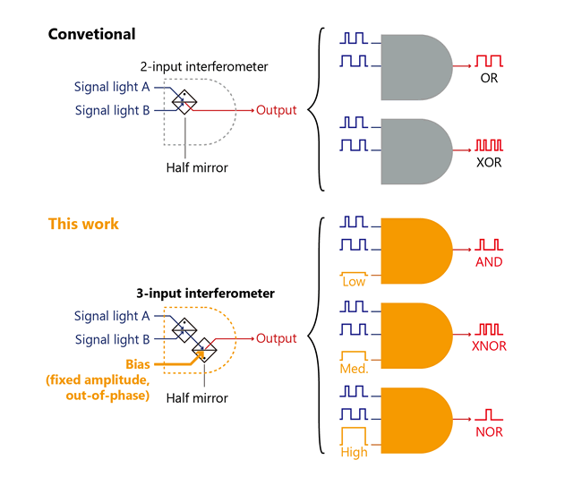
Therefore, in this study, we have realized “a high-performance ultralow-latency optical logic gate*5 based on light-interference” for the first time in the world. The light-interference is a “linear” phenomenon, so originally it is too simple to do many logic operations, and the function is limited. However, we have found that almost all representative Boolean logic operations can be performed with a single nanophotonic gate by introducing our new idea of “Bias” light with adjusting the input conditions (Fig. 2). We have also tried to find a newly shaped nanophotonic gate based on silicon photonics technology*6, then we have realized the following achievements.
Achievements
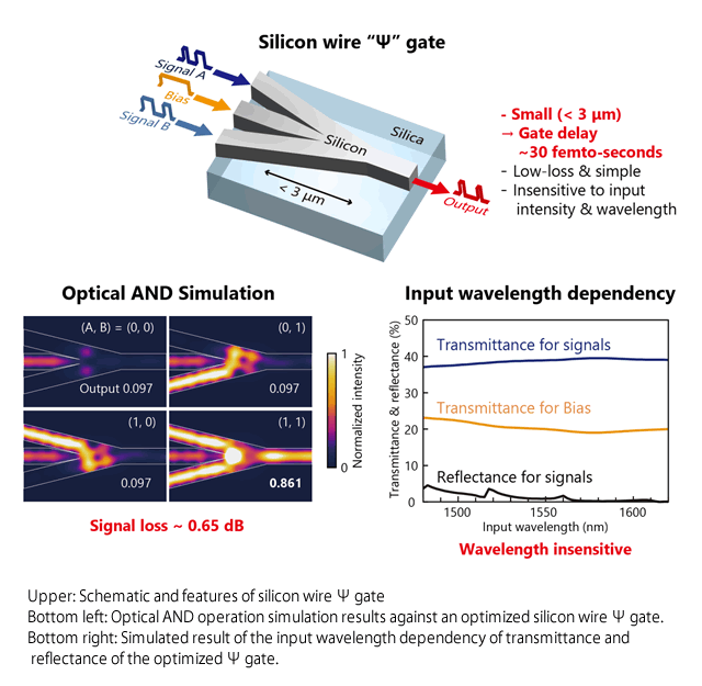
Our research group has simulated and found a 3-µm long, low-loss, and simple silicon wire Ψ (psai) gate by assuming the device structure with thin film silicon layer on dielectric (silica) substrate (upper side of Fig. 3). By fabricating this, we have experimentally demonstrated low-loss, high-speed, and wavelength independent Boolean logic operations for the first time in the world. Mainly, there are three related achievements as following;
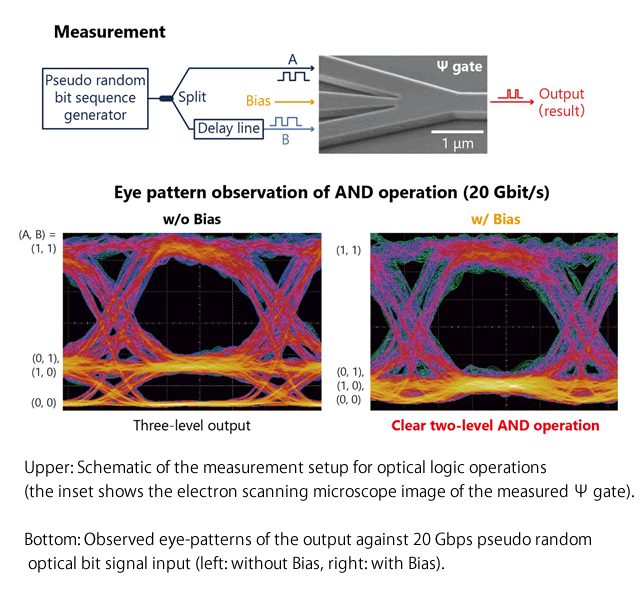
- Low-loss and high-speed logic operation by a silicon wire Ψ gate
We fabricated silicon wire Ψ gates which were optimized through multiple optical wave simulations, and we put two pseudorandom optical signal bit patterns (A and B), and one continuous wave input (Bias) to the fabricated Ψ gate (upper side of Fig. 4). As the result, we have observed clear optical AND operation by introducing the Bias light with appropriate amplitude (bottom side of Fig. 4). It is the first time in the world to observe such high-speed and clear AND operation based on light-interference, and it was produced by the low insertion loss of the silicon wire Ψ gate. From the devise size, the operation latency can be estimated to only ~30 femto-seconds (ten to the minus fifteen-seconds) It is ~10 pico-seconds (ten to the minus twelve-seconds) for general electronic circuits. Therefore, Ψ gates are ~300 times lower-latency than conventional electronic logic gates. - Switching to the other optical logic operation function in a single gate
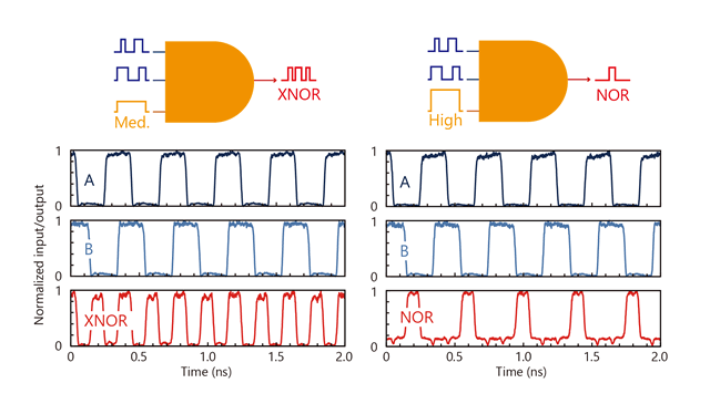
We have succeeded to switch the logic operation from AND to XNOR (left side of Fig. 5) or NOR (right side of Fig. 5) by appropriately increasing the input amplitude of the Bias light against the above same device. This is also the first observation in the world as well as the above AND operation. - Input wavelength insensitive optical logic operation
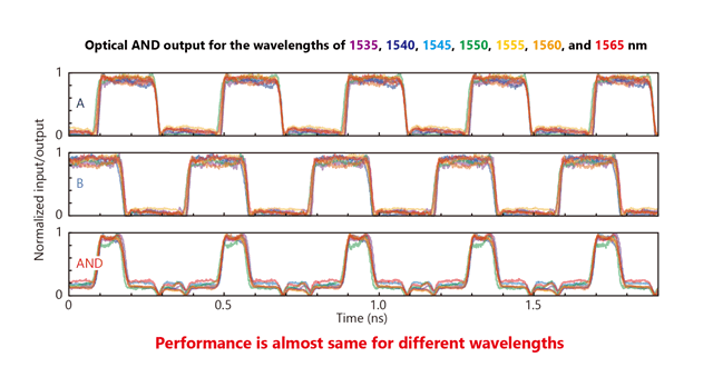
We have also confirmed that the above same device can operate almost same AND function even with different input wavelengths Fig. 6). If we input those different wavelengths simultaneously, we can finally perform so called “wavelength multiplexed parallel operation” by assigning the different bit patterns and different operation functions to each wavelength channel because there is almost no mutual interaction among the different wavelengths. This is one of the operations that is very difficult for nonlinear optical gates.
Outlook
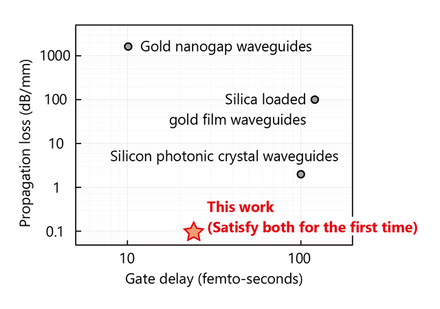
The above demonstrated silicon wire Ψ gate is the world-first optical logic gate that can overcome the conventional trade-off between the small device size and the low insertion loss (Fig. 7). The Ψ gate suggests the new potential of the optical processing technology that may essentially solve the latency bottle-neck of the conventional electronic circuit technology. Therefore, it is expected to be one of elemental devices for photoelectric converged data processing infrastructures in the future. For example, it is possible to realize ~10 times lower latency multi bit (128-bit) AND operations than the case of conventional technologies by cascading the silicon wire Ψ gates like a tree. If we integrate a bunch of wavelength–selective high speed optical modulators with the cascaded Ψ gates, we can perform larger scale multi bit AND operations, and wavelength multiplexed parallel operations that can realize the independent operation for each wavelength channel. Moreover, both latency and loss could be improved by utilizing multi input Ψ gates more than current three, but five, seven, and maybe more.
In the near future, this technology may support much safer data communication by applying to a part of pattern matching processing against header information of the read-out optical bit sequence in optical routers. It is also possible to apply to high speed pattern matching processing for big data such as DNA sequences. Actually, multi input Ψ gates could be also useful to achieve lower latency and lower energy consumption photonic neural network accelerators*7, because Ψ gates perform vector operations naturally.
Technical points in detail
- Logic operations by light-interference
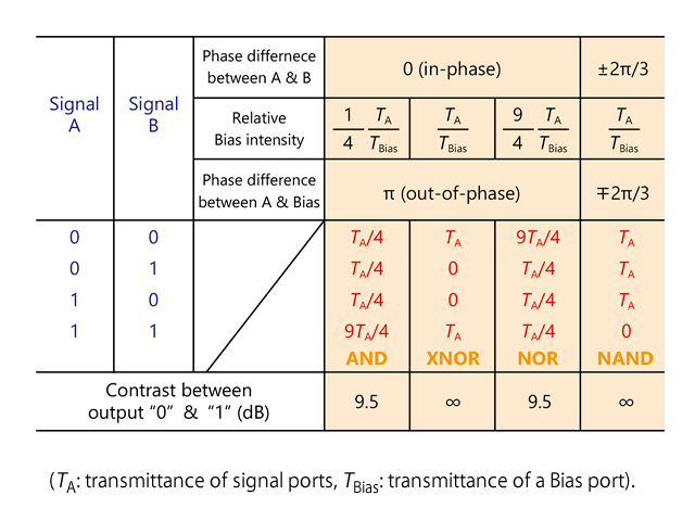
We have found that various optical logic operations can be done a 3-input interferometer with assuming 3 inputs – two signal lights A and B, and one more “Bias” light with fixed amplitude, plus each phase relationship is properly controlled (Fig. 8). Notably, the function among AND/XNOR/NOR can be switched by only changing the amplitude of the Bias light. The signal contrast between logic “0” and “1” levels can be larger than 9.5 dB including NAND operation. The signal loss is defined as the ratio between the single input and the output intensity for logic “1” level. Therefore, the signal loss can be more reduced by increasing the transmittance of the signal ports. Once the transmittance of the signal ports becomes larger than 4/9, the signal loss becomes less than zero. However, please note that there is one critical constrain – the summation of the transmittance of the single interferometer must be less than one. Therefore, if we set the transmittance of the signal ports to too high value, this makes the transmittance of the Bias port too small, so the required intensity of the Bias light for the clear logic operation becomes too high. So we should balance and design both transmittances with considering all the necessary optical input intensity including the Bias light (corresponding to the relative operation energy). - Invention of a small and low-loss silicon wire Ψ gate
We have found that a 3-µm long silicon wire Ψ gate that resembles a Greek letter of ”Ψ” as a 3-input 1-output coherent optical combiner based on silicon photonics technology (upper side of Fig. 3). It has been also found that this gate can perform quite low-loss optical AND logic operation by optimizing the waveguide structures such as the waveguide angle, taper width, taper length and so on (bottom left side of Fig. 3). One large advantage of this gate is that the performance of the logic operation is quite insensitive to how large input intensity and which input wavelength. It is also found that the signal reflection can be reduced more than our expectation by forming narrow gaps at the waveguide crossings (bottom right side of Fig. 3). The balancing of transmittance between the signal and Bias ports is also flexibly done with tuning the structural parameters.
Publication information
fff
Journal: Communications Physics
Title: Ultrashort low-loss Ψ gates for linear optical logic on Si photonics platform
Authors: Shota Kita, Kengo Nozaki, Kenta Takata, Akihiko Shinya, and Masaya Notomi
Glossary
- *1 ... CMOS electronics technology
- CMOS is a technology for constructing electronic transistors that is also used in electronic digital logic circuits. The advantages of CMOS, which include a low fabrication cost and low energy consumption, mean that it is widely used in large-scale microprocessors with dense integration. Its miniaturization and dense integration have developed in accordance with Moore’s law. However, this development is gradually approaching its physical limit as regards fabrication and saturation in terms of energy consumption.
- *2 ... Nano photodetectors
- Drastically miniaturized photodetectors achieved by putting the absorber in photonic crystal waveguide whose structure is periodically modulated as small as light wavelength scale. Owing to the small electric capacitance of less than one femto-farad, it can keep > 10 GHz bandwidth even with using relatively large load resistance of 10 kilo-ohm order. Then low energy consumption and low noise photo receiving operation without a transimpedance amplifier becomes possible.
- *3 ... Nanophotonic modulators
- Drastically miniaturized and low energy consumption optical modulators based on nano-scale optical cavity formed by photonic crystal.
- *4 ... Optical transistors
- By connecting a nano photodetector and a nanophotonic modulator electrically, the nanophotonic modulator can be driven by the generated voltage at the nano photodetector. Therefore, another light input to the nanophotonic modulator can be modulated only by the input light to the nano photodetector (pseudo optical nonlinear gate hidden by the low capacitance electronics). Amplification (increasing the output signal amplitude than the input) like transistors is also possible, so it is an optical transistor.
- *5 ... Optical logic gates
- Optical gates realizing or imitating Boolean logic operations (AND, OR, etc.) used in digital electronics. There are many ideas based on nonlinear optical gates, however the nonlinear optical effect is intrinsically too small and there is a general trade-off between the gate length and the insertion loss. For now, it is very difficult to compose optical processing circuits only by optical nonlinear gates without degrading the potential of low latency operation.
- *6 ... Silicon photonics
- One maturing photonic device system based on narrow silicon wire waveguides whose principle is the optical confinement by total internal reflection in high index contrast structures. By forming heaters or p-n junctions with doping impurities, many optical phase modulators can be integrated on a same chip. The uniformity of the device has been drastically improved by employing 300 mm process by using Si CMOS pilot lines, thus quite larger scale optical matrix switch has become available recently.
- *7 ... Neural network accelerators
- High efficiency and high speed processors specialized for some deep learning applications. The electronic circuit architecture imitates the operation of neural networks like human brains, so it is called a sort of artificial neural networks. For now, many research groups try to demonstrate photonic neural network accelerators with various types of photoelectric converged circuit architecture. The operation energy can be much more efficient because all the vector operations can be embedded by using light-interference – it is said that ~90% of energy is consumed due to the vector operations in conventional neural network accelerators.


