


The world's first demonstration of aluminum nitride transistor
- Advancing toward next-generation power devices contributing to carbon neutrality -
Tokyo-April 22, 2022ーNTT Corporation (TYO: 9432), today, announces that it has achieved transistor*1 operation using high-quality aluminum nitride (AlN). Transistors, which are an essential component of semiconductor power devices*2, are used for power conversion in home electronics and electric vehicles, and their improved efficiency will contribute to energy saving. AlN for ultra-wide bandgap (UWBG) semiconductors*3 has a large breakdown field and is therefore a promising semiconductor material for achieving low-loss, high-voltage power devices. NTT has successfully produced high-quality AlN by using metalorganic chemical vapor deposition (MOCVD)*4 and also developed formation methods of ohmic*5 and Schottky*6 contacts. These technologies allowed us to demonstrate AlN transistors for the first time. Furthermore, even at the high temperature of 500°C, the AlN transistors showed good device characteristics. These results will contribute to realization of ultra-low-loss power devices and high-temperature electronics.
=> Press Release
=>Thin-Film Materials Research Group
Background
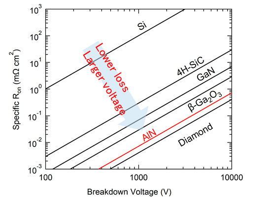
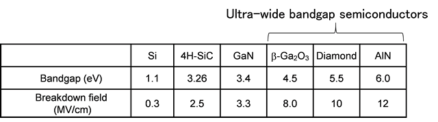
Semiconductor power devices utilized for power conversion are widely used in home electronics, PCs and smartphones, as well as database servers and electric vehicles. In recent years, applications of power devices have expanded to high-power operation such as photovoltaic power generation and railways. In the quest to achieve carbon neutrality, the loss of power devices should be reduced even further. Silicon (Si) is commonly used for semiconductor power devices. By using a wide bandgap semiconductor with a large breakdown field, it is possible to reduce the loss and increase the breakdown voltage. Therefore, wide bandgap semiconductors such as silicon carbide (SiC) and gallium nitride (GaN) are being developed for power devices. UWBG semiconductors with a breakdown field larger than that of SiC or GaN further improve the performance of power devices (Fig. 1). UWBG semiconductors include AlN, diamond, and gallium oxide (Ga2O3) (Table I). For AlN power devices, the power loss is theoretically expected to be only 5% of Si, 35% of SiC, and 50% of GaN.
AlN has been used as an insulator since it was first synthesized more than a century ago. In 2002, NTT succeeded in fabricating semiconducting AlN for the first time in the world, thus opening up new avenues in semiconductor device applications. Among UWBG semiconductors, AlN is advantageous in that devices can be fabricated on large-scale wafers and various device structures can be obtained by heterojunction formation with other nitride semiconductors such as GaN. However, there have been few reports on power device fabrications in this vein, and their characteristics need to be improved.
Results
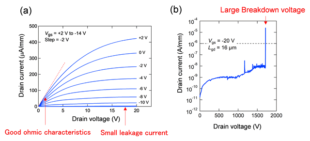
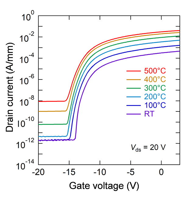
NTT succeeded for the first time in transistor operation with good characteristics using a high-quality semiconducting AlN fabricated by MOCVD. The current-voltage characteristics of the AlN transistors showed good ohmic characteristics (Fig. 2 and 3) and an extremely small leakage current. The breakdown voltage was as large as 1.7 kV. We also confirmed that the AlN transistor can operate stably at high temperatures (Fig. 4). In contrast to conventional semiconductor materials, AlN transistors showed improved performance at high temperatures. The drain current increased to about 100 times as ambient temperature increased from room temperature to 500°C. Moreover, even at 500°C, the leakage current was kept extremely low at 10-8 A/mm. As a result, a high drain current on/off ratio of 106 was obtained at 500°C.
Technical points
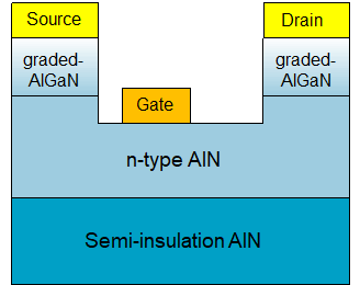
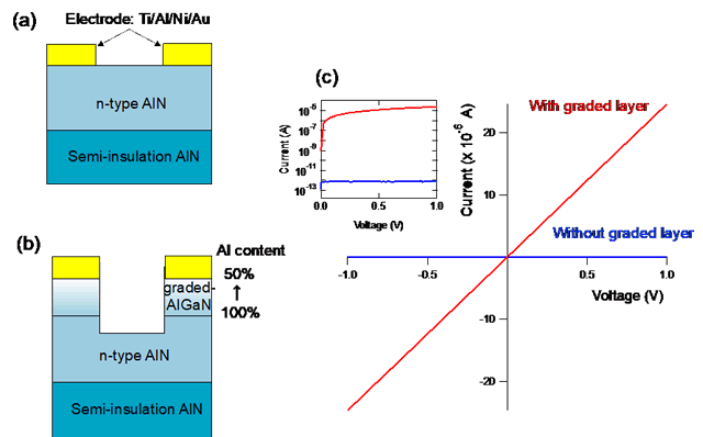
The first technical point to address is the crystal growth technique for high-quality AlN. The density of residual impurities and crystal defects in AlN has been reduced by developing a unique high-temperature MOCVD with a specially designed reactor. As a result, NTT has achieved a high-quality n-type AlN semiconductor with the world's highest electron mobility. The second point is how to achieve good ohmic contacts. AlN has large energy barriers to metals, making it difficult to form ohmic contacts on it. NTT used a compositionally graded AlGaN layer between AlN and metal electrodes in order to obtain good ohmic contacts (Fig. 5). The third point is how to achieve Schottky contacts with good rectification. Schottky characteristics are affected by the crystal quality of the semiconductor, the interface state between the semiconductor and metal electrodes, and the contact resistance of the ohmic electrode. As stated above, owing to high-quality AlN and good ohmic contact, NTT has achieved nearly ideal Schottky characteristics with good rectification.
The establishment of these elemental technologies led to the successful operation of the AlN transistors.
Future developments
In the quest toward ultra-low-loss power devices and high-temperature electronics, NTT will further improve the performance of AlN-based power devices and investigate the device operation at high temperatures.
Publication Details
Title: High-Temperature Performance of AlN MESFETs With Epitaxially Grown n-Type AlN Channel Layers
Authors: M. Hiroki, Y. Taniyasu and K. Kumakura
Journal: IEEE Electron Device Letters
Publication Date: 07 January 2022
DOI: 10.1109/LED.2022.3141100
Glossary of terms
- *1 ... Transistor
- A three-terminal semiconductor device used to amplify electrical signals or switch electrical power.
- *2 ... Semiconductor power device
- A semiconductor device used in power electronics for power conversion.
- *3 ... Ultra-wide bandgap (UWBG) semiconductor
- Bandgap is the main material parameter that determines semiconductor properties. Semiconductors with a larger bandgap energy have a higher breakdown field. The bandgap energy of Si is 1.1 eV. Semiconductors with a large bandgap energy of about 3 eV, such as SiC and GaN, are called wide bandgap semiconductors. AlN, Ga2O3, and diamond have larger bandgap energies than SiC and GaN, and are therefore called UWBG semiconductors
- *4 ... Metal-organic vapor phase epitaxy (MOCVD)
- A method for growing thin-film crystals. Organic metal and gas are used as sources. A thin-film crystal is grown on a heated substrate via chemical reaction of the sources.
- *5 ... Ohmic contact
- Metal/semiconductor contacts in which the current varies linearly with applied voltage following Ohm's law.
- *6 ... Schottky contact
- Metal/semiconductor contacts that exhibit rectification property.


