


Realizing Zero-bias Operation of a Graphene Photodetector at 220 GHz and Elucidating the Optical-to-electrical Conversion Process
~Demonstrating the Promise of Graphene as a Broadband High-Speed Photodetector Material~
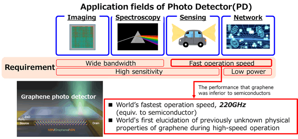
NTT Corporation (NTT; Head Office: Chiyoda-ku, Tokyo) and the National Institute for Materials Science (NIMS) have jointly achieved the world's fastest zero-bias operation*1 (220 GHz) of a graphene photodetector (PD)*2. Furthermore, they clarified the optical-to-electrical (O-E) conversion process in graphene for the first time. Graphene is expected to have high sensitivity and high-speed electrical response to a wide range of electromagnetic waves, from terahertz (THz) to ultraviolet (UV). Thus, it is a promising PD material to enable high-speed O-E conversion at wavelength ranges where existing semiconductor devices cannot operate. However, until now, the demonstrated operating speed under zero bias has been limited to 70 GHz by device structure and measurement equipment problems. For this reason, the intrinsic properties of graphene have not been investigated, and the principle of PD operation has not been elucidated.
In this study, we demonstrated an operating speed of 220 GHz by removing the current delay caused by the device structure and by using on-chip THz spectroscopy technology to read out the current at high speed. We also found that there is a trade-off between operating speed and sensitivity. Furthermore, we succeeded in elucidating the O-E conversion process in graphene. The findings will enable graphene PDs to be optimized according to their intended use, such as optical sensors prioritizing sensitivity or O-E signal converters prioritizing speed. The research is published online in the British scientific journal Nature Photonics on 25 August 2022.
=> Press Release
=> Quantum Solid State Physics Research Group
Summarization figure of this result
Background of the Study
Photodetectors (PDs), which convert optical signals into electrical signals, are key devices in communications equipment and sensors. In particular, realization of efficient information technology will require PDs that operate at high speed on a wide bandwidth for optical sensors that operate in various wavelength regions and wideband communications that exceed the bandwidth limitations of existing technologies. Graphene is a promising material for meeting these requirements. Previous research on graphene PDs has shown that they can operate over an ultra-broad frequency range *3 from THz to ultraviolet and absorb 2.3% of light with only one atomic layer, making them highly efficient. On the other hand, their demonstrated operating speed under zero bias has been limited to 70 GHz because of problems with the device structure and measurement equipment, falling far short of the theoretical expectation of exceeding 200 GHz. Also, due to these issues, the intrinsic response of graphene has not been investigated. Therefore, the challenge for graphene PDs is to demonstrate 200-GHz operation speeds and clarify graphene's inherent properties, such as the process by which optical signals are converted into electrical signals.
Research results
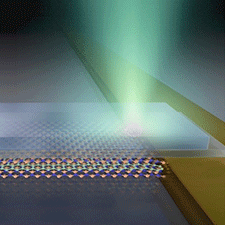
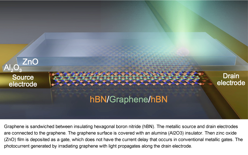
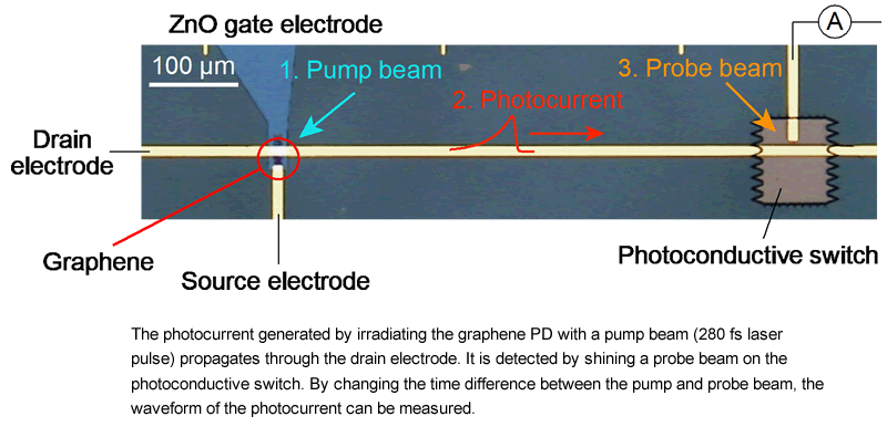
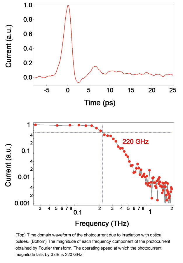
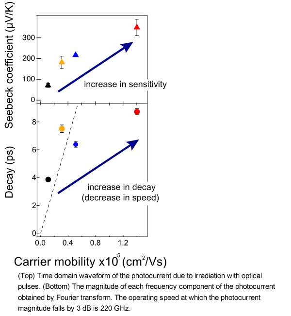
Our research group has studied O-E conversion in graphene, focusing on the photothermoelectric (PTE) effect *4, which enables zero-bias operation required for applications with constraints on power consumption and signal-to-noise ratio. In the PTE effect, an electric current flows according to the electron temperature in graphene, which is raised by irradiating the material with light. The keys to achieving high-speed O-E conversion are a device structure that allows the current to follow the ON/OFF cycle of the light irradiation without delay and technology to read out the current at high speed. The current delay caused by electrostatic coupling between graphene and the gate is eliminated by using zinc oxide (ZnO) thin film as the gate material instead of commonly used metallic materials such as gold (Key Technology Points (1) and Figure 1). On-chip THz spectroscopy was used to read out the current at high speed (Key Technology points (2) and Figure 2). As a result, we demonstrated high-speed operation with a 3dB bandwidth of 220 GHz, as expected theoretically (Figure 3). We found a trade-off between operating speed and sensitivity by comparing the characteristics of PDs fabricated with graphene of different qualities (Figure 4).
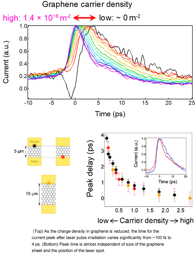
Furthermore, we elucidated the O-E conversion process in graphene. In particular, we showed that, contrary to conventional understanding, the response time of the current is almost independent of the size of the PD. Moreover, the time from light irradiation to current generation can be varied significantly from less than 100 fs to more than four ps, depending on the carrier density (Figure 5). These results are not only academically significant, but also essential for designing graphene PDs for information processing, sensors, and other applications.
Key Points of the Technology
(1) The resistivity and other properties of ZnO thin films vary depending on the deposition temperature. By using an appropriate deposition temperature, it is possible to apply DC voltage and at the same time make the film insulating to high-frequency electromagnetic fields. By using ZnO thin film as a gate, the current delay caused by the capacitive coupling between graphene and the gate material is avoided.
(2) The THz current generated by photoexcitation of graphene is detected on-chip, by using a photoconductive switch to achieve a measurement bandwidth around 1 THz. This technique overcomes the limitation of the conventional method of measuring high-frequency currents with electronic devices such as oscilloscopes, which has a measurement bandwidth of around 100 GHz.
Future Developments
The results of this study demonstrate the potential of graphene as a high-speed broadband PD. However, the graphene in this experiment was exfoliated from graphite, meaning that it is unsuitable for mass production. In general, the quality of graphene deposited over a large area is inferior to that obtained by exfoliation. However, the gap in quality is shrinking year by year thanks to advances in deposition technology. In the future, we will evaluate PDs using large-area graphene that can be mass produced.
In addition, research has been active in creating materials that do not exist in nature by layering graphene and other two-dimensional materials (single or multi-layered atomic layer materials). We will search for materials that can achieve even faster operation by thoroughly using this technology.
Publication Information
Nature Photonics
Title: “Ultrafast intrinsic optical-to-electrical conversion dynamics in a graphene photodetector”
Authors: Katsumasa Yoshioka, Taro Wakamura, Masayuki Hashisaka, Kenji Watanabe, Takashi Taniguchi, and Norio Kumada
Figure: Experimental system for graphene photodetector measurement
Terminology
- *1 ... Photodetector (PD)
- A device for electrically detecting light by converting optical signals into electrical signals. Generally, semiconductors such as silicon and germanium are used for PDs.
- *2 ... Zero bias operation
- An operation in which no voltage is applied between the source and drain electrodes. In graphene, in particular, applying a source-drain voltage causes a large current to flow, so zero-bias operation is essential from the standpoint of power consumption and signal-to-noise ratio.
- *3 ... Ultra-wide bandwidth
- General semiconductor PDs are not sensitive to light with long wavelengths (>1 µm for silicon) because they cannot absorb light below the material's intrinsic bandgap. On the other hand, graphene is known to be sensitive to THz waves (wavelength: ~1 mm) because of its zero-bandgap electronic structure.
- *4 ... Photothermoelectric effect
- The thermoelectric effect is a phenomenon in which voltage is generated when a temperature difference is applied to a junction of materials with different Seebeck coefficients (a coefficient that expresses the relationship between temperature and voltage). In particular, when the temperature is changed by irradiating the material with light, it is called the photothermoelectric effect. In the case of graphene, the Seebeck coefficient varies with the charge density. In this research, the photothermoelectric effect is caused by forming a region of different charge density near the interface with the electrode.


