Hiroyuki Tamura1, and Tatsushi Akazaki1
1Physical Science Laboratory,
2University of Tsukuba/NTT Research Professor, 3Tohoku University
A high-quality low-density two-dimensional electron system (2DES) in semiconductors
can be formed on gated undoped GaAs quantum wells (QWs) grown by molecular
beam epitaxy. Some interesting phenomena, such as Wigner crystallization,
are predicted to appear in low-density 2DES theoretically because the large
Coulomb interaction between electrons plays a role. However, the unavoidable
potential randomness in real samples disturbs the ideal 2D condition. Investigating
the screening of the potential randomness by the induced electrons would
therefore help us to better understand the low-density 2DES properties.
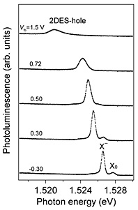
In this study, we performed photoluminescence (PL) measurements on an
undoped GaAs QW for different electron densities with a gate bias. We found
a two-stage transition reflecting the change of the potential-screening
properties when the electrons were induced [1]. By PL measurement, we can
seamlessly follow the transition from the insulating to the metallic regimes
through the PL spectrum change from the exciton (X0) and charged excion (X-) to the 2DES-hole recombination. The typical PL spectra are shown in Fig.
1 from the bottom to top with increasing gate bias voltage. The two-stage
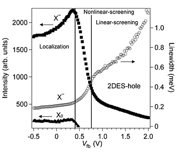
change of PL intensity and linewidth against the gate bias voltage, shown
in Fig. 2, corresponds to the transition from the electron localization
in the insulating regime to the linear screening in the metallic regime
through a non-linear screening regime. In the linear screening regime,
the induced electrons effectively screen the random potential, whereas
the electrons partially screen the random potential valley in the non-linear
screening regime. The randomness of our sample may originate from electrons
trapped in the surface state. A sample with a larger distance from the
surface to the QW may reduce the random potential at low electron density.
This work was partly supported by CREST program of Japan Science Technology
Agency.
[1] M. Yamaguchi et al., Phys. Rev. Lett. 100 (2008) 207401.
 |
 |
|||||
|
|