Shintaro Nomura3, and Hideaki Takayanagi4
1Physical Science Laboratory, 2University of Tsukuba,
3University of Tsukuba/NTT Research Professor, 4Tokyo University of Science
InGaAs-based heterostructures with a large Rashba spin-orbit interaction are very attractive for applications in semiconductor spintronics [1]. In terms of spin manipulation, it is very important to investigate the optical effect on the transport properties in these InGaAs-based heterostructures. This is because spin-aligned carriers are generated when electrons are excited by circularly polarized light. In this study, we investigated the transport of a two-dimensional electron gas (2DEG) in an In0.52Al0.48As/In0.7Ga0.3As heterostructure when exposed to light from infrared laser diodes (λ=0.78, 1.3 µm) [2].
In the dark, the sheet carrier density nHall and mobility µ of the 2DEG at 1.8 K obtained with Hall-effect measurements
were found to be 〜2.3×1012 cm-2 and 〜161,000 cm2/Vs, respectively. To investigate the optical effect, the laser light was
guided through an optical fiber close to the surface of a Hall-bar sample
placed in a magnetic field of 0.5 T at 1.8 K. The Hall voltage was measured
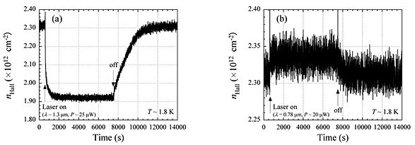
before, during and after illumination. The nHall was estimated using the measured Hall voltage. Figure 1 shows the time
dependence of nHall before, during and after illumination with (a) 1.3 µm and (b) 0.78 µm light. When the sample was illuminated with 1.3 µm light, nHall immediately decreased and became constant, although photo-induced carriers
were generated in the In0.7Ga0.3As channel layer. After the illumination was switched off, nHall slowly increased and regained its initial value after about one hour.
In contrast, when the sample was illuminated with 0.78 µm light,
nHall increased slightly only during illumination. We concluded that negative photoconductivity occurs in In0.52Al0.48As/In0.7Ga0.3As heterostructures when they are illuminated by photons with λ=1.3 µm, namely at the longer wavelength (lower energy), in contrast to several previous reports stating that negative photoconductivity in InAs/AlSb heterostructures occurs only when they are illuminated by photons with a relatively high energy [3]. We would speculate that the negative photoconductivity in In0.52Al0.48As/In0.7Ga0.3As heterostructures is attributed to the presence of the deep impurity
levels in the In0.52Al0.48As layer.
This work was partly supported by CREST program of Japan Science Technology
Agency.
[1] J. Nitta et al., Phys. Rev. Lett. 78 (1997) 1335.
[2] T. Akazaki et al., Physica E 40 (2008) 1341.
[3] Yu. G. Sadofyev et al., Appl. Phys. Lett. 86 (2005) 192109.
 |
||
|