Materials Science Laboratory, *Keio University
Brain-machine interfaces that link the brain and the external world have
been developed in the neuroscience and medical fields. Most of these interfaces
are designed for one-way communication; however we have developed an interface
that makes two-way communication possible through a microelectrode array
(MEA)[1]. The electrical stimulation of the brain and neural activity measurement
are important in relation to this communication, as is the interpretation
of information in the brain. Furthermore, an unwired and miniaturized device
is desirable in terms of reducing the stress induced when the device is
worn on the body. In this study, we have developed 16-ch preamplifiers
with multi-channel stimulation circuits on a 2.5 mm × 1.4 mm LSI chip using
a 0.18 µm CMOS process [2].
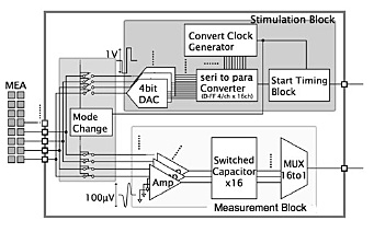
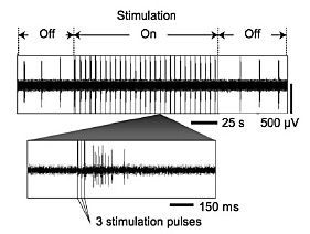
Figure 1 shows the three main components of this LSI chip: a stimulation block, a measurement block and a mode change block. The stimulation block can produce a 16 ch 4-bit parallel arbitrary waveform by combining 10 µs-wide pluses for electrical stimulation. The measurement block has 16 ch pre-amplifiers, and a multiplexer to combine 16 ch neural signals into one signal at a sampling rate of 40 kS/s. The mode change block switches between the stimulation and measurement blocks when it receives a control signal generated by the stimulation block. Figure 2 shows the neural activity of dissociated rat cortical neurons on the MEA with and without stimulation. A few tens of milliseconds after applying three stimulation pulses to one electrode, neural activity was observed with a different electrode.
We will unwire the input and output between this LSI chip and the external unit to improve the portability of the device as a brain-machine interface.
[1] A. Shimada et al., SFN 2008, Washington, D.C. U.S.A. (Nov. 2008).
[2] M. Yamaguchi et al., Jpn. J. Appl. Phys. Accepted.
 |
 |
|||||
|
|