Quantum Transport in Silicon-On-Insulator Structures
Å@
Kei Takashina, Yukinori Ono, Akira Fujiwara, Yoshiro Hirayama*, and Toshimasa Fujisawa
Physical Science Laboratory
Å@Besides being of immense technological importance, electrons in silicon
offer a number of unique possibilities for exploring new physical conditions
and new phenomena. One of these arises due to their bulk dispersion relation
where there are six, energetically degenerate conduction band valleys.
In Si(100)-MOSFETs where electrons are two-dimensionally confined, this
six-fold degeneracy is lifted, due to anisotropic effective mass, to leave
only two low lying valleys available for occupation. 2-D electrons in such
structures consequently have freedom as to how they occupy these degenerate
valleys giving them a valley degree of freedom on top of in-plane motion
and spin.
Å@In the present study, we have been able to show that valley-splitting,
which lifts this remaining two-fold valley degeneracy can be enlarged and
controlled over an unprecedented extent using SOI (Silicon-On-Insulator)
MOSFETs [1] and that its effects can be observed clearly by direct transport
measurements even without magnetic field (Figures) [2]. The results demonstrate
considerable potential for exploring valley-related phenomena and new device
possibilities.
[1] K. Takashina, A. Fujiwara,
S. Horiguchi, Y. Takahashi, and Y. Hirayama, Phys. Rev. B 69 (2004) 161304(R).
[2] K. Takashina, Y. Ono, A. Fujiwara, Y. Takahashi, and Y. Hirayama, Phys.
Rev. Lett. 96 (2006) 236801.
*Present address: Tohoku University
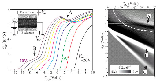 |
| Fig. 1. |
Two-terminal conductance at 4.2K as a function
of front-gate voltage VFG
at various values of back-gate voltage VBG.
The inset shows the experimental setup. A and B mark features associated with
second-confinement-subband occupation and valley splitting respectively. Right:
2nd derivative of the data showing the evolution of the features. The white
squares joined by lines mark self-consistently calculated positions of the
onset of second-confinement-subband occupation using nominal parameters of the
device. (The feature marked C is due to the onset of conduction.) |
|
[back]Å@[Top]Å@[Next]