Materials Science Laboratory
The thermal chemical vapor deposition (CVD) method has been widely used
to grow single-wall carbon nanotubes (SWNTs). However, direct growth of
doped SWNTs and tuning of the impurity concentration in them are still
a big challenge. Another very important issue for doped SWNTs is their
characterization. In particular, it is very difficult to evaluate carrier
concentrations in individual SWNTs. Thus, the carrier concentration has
not been clarified in previous studies of doped SWNTs. In this study, we
grew boron (B)- and nitrogen (N)-doped SWNTs from B- and N-containing feedstocks
by the thermal CVD method. Raman spectral shifts induced by carrier doping
were clearly observed and the carrier densities were evaluated from the
shifts [1].
We used triisopropylborate (C9H21BO3) and benzylamine (C7H9N) as B- and N-containing feedstocks. These chemicals also acted as a carbon
source, and we did not use any other carbon sources. B- or N-doped SWNTs
were grown from either one or the other feedstock, with a Co thin film
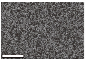
deposited on a SiO2/Si substrate used as a catalyst. We were also able to synthesize BN-doped
SWNTs by supplying both triisopropylborate and benzylamine simultaneously,
as shown in Fig. 1. Transmission electron microscopy and Raman (radial
breathing mode) measurements indicated that the diameter of the doped SWNTs
is mostly 1-2 nm, like that of undoped SWNTs grown using a similar catalyst.
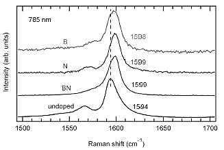
Figure 2 shows Raman (G band) spectra of B-, N-, and BN-doped SWNTs, and
undoped SWNTs. As can be seen in the figure, the G band position in the
doped SWNTs is shifted to the high-wavenumber side by 3-6 cm-1, regardless of the choice of feedstock. The hardening of the G band regardless
of doping type (electron or hole doping) can be understood as renormalization
of phonon energy through electron-phonon coupling induced by a Fermi level
shift in a semiconducting SWNT. Originally, the energy of the G band phonon
is softened by the electron-phonon interaction (Kohn anomaly). However,
a Fermi level shift reduces the electron-phonon interaction and thus, reduces
the effect of the Kohn anomaly. Consequently, the Fermi level shift induced
by electron or hole doping causes a hardening of the G band. The G band
hardening is expected to become prominent when the Fermi level reaches
the valence or conduction band. Therefore, the results shown in Fig. 2
indicate that the Fermi level in the doped SWNTs is located inside the
valence or conduction band. We can also estimate the carrier density. Assuming
that the SWNT diameter is 1.5 nm, the estimated carrier concentration reaches
0.4-0.8%, which is a considerably large value.
[1] S. Suzuki and H. Hibino, Carbon 49 (2011) 2264.
 |
 |
|||||
|
|