1Materials Science Laboratory, 2Physical Science Laboratory, 3The University of Tokushima
Monolayer and bilayer graphene have gained significant attention because
of their potential applications for high-frequency devices and for logic
devices, respectively. The mechanical exfoliation of graphite is a common
way of making graphene because high-quality graphene can be obtained. However,
this technique is only good for making graphene flakes of only a few tens
micrometers in size. For wafer-scale synthesis of graphene, we employ thermal
decomposition of SiC, which enables epitaxial growth of graphene layers.
By annealing SiC(0001) in an Ar atmosphere and in an UHV environment, we
have succeeded in growing monolayer and bilayer graphene, respectively.
To elucidate the transport properties of these graphene, we systematically
studied the electrical properties of monolayer and bilayer graphene in
top-gate devices.
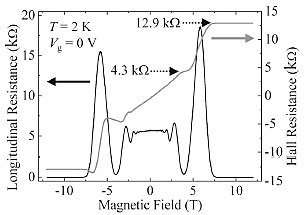
Figure 1 shows the magnetic-field dependences of longitudinal resistance
and Hall resistance of the monolayer-graphene device. The magnetic field
was applied perpendicular to the graphene plane. The Hall resistances become
constant as a function of magnetic field at the resistances unique to monolayer
graphene, where, at the same time, the longitudinal resistances show minima.
At high-magnetic field, the minimum resistance of the longitudinal resistance
becomes zero, which is a hallmark of the quantum Hall state. By decreasing
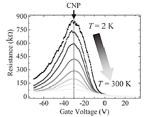
the carrier density with applying gate voltage (Vg), the mobility increases, and the mobility at 2 K exceeded 10,000 cm2 V-1 s-1 at a carrier density of 3×1010 cm-2, which is comparable to that of exfoliated graphene transferred onto SiO2 [1]. Figure 2 shows the gate-voltage dependence of resistance of the bilayer-graphene device from 2 to 300 K. In all temperatures, resistance at the charge neutrality point (CNP) shows maximum resistance [2]. The strong temperature dependence of the resistance at the CNP results from band gap opening due to the interaction of the graphene with the substrate. The observed quantum Hall effect in the monolayer-graphene device proves high quality of the monolayer graphene and the electrical detection of the band gap in bilayer-graphene device is an important finding for its applications. These results show that the thermal decomposition of SiC is an effective method to grow monolayer and bilayer graphene.
This work was supported by KAKENHI.
[1] S. Tanabe et al., Appl. Phys. Express 3 (2010) 075102.
[2] S. Tanabe et al., Jpn. J. Appl. Phys. 50 (2011) 04DN04.
 |
 |
|||||
|
|