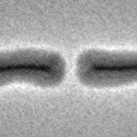
- Scanning electron microscopy (SEM) image of Si single-electron
device. Si nanostructure embedded
in oxide is clearly observed by secondary electron mode.
more information -> poster presentation for MNE99
| ■ ■ ■ SEM image of SED ■ ■ ■ |
|
|
|
more information -> poster presentation for MNE99 |
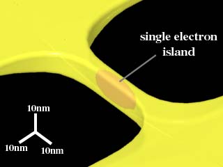
| ■ ■ ■ 3D modeled structure of SED ■ ■ ■ |
 |
|
RETURN to previous page