1 MHzの超高繰返し動作で1.7サイクル高強度パルス光の発生に成功 ~次世代の高輝度アト秒パルス光源の実現に向けて~
https://doi.org/10.1364/OL.477372[English]
T. Okamoto1, Y. Kunihashi1, Y. Shinohara1, H. Sanada1, M. -C. Chen3, K. Oguri1
1 NTT Basic Research Laboratories, Japan
2 Institute of Photonics Technologies, National Tsing Hua University, Taiwan
 Fig. 1. 本研究で構築したマルチプルプレート圧縮器
光の波の1.7周期しか時間幅を持たない非常に短い光パルスを、極めて高い繰り返しレート*1(1 MHz = 1秒間に10万回、従来よりも数百倍速いレート)で発生させることに成功しました。イッテルビウム(Yb)系固体レーザーにマルチプルプレート法*2という技術を適用することで実現したこの光源は、大規模なレーザーシステムや冷却機構を必要としない簡便なセットアップで構成されているにも拘わらず、世界最高クラスの性能を有します。本手法を用いれば、世界で限られた施設でしか発生できなかったMHzレベルの高繰返し高強度レーザー光源を、より簡便に低コストで利用できるようになることから、超高速現象や超高強度光技術等の多岐に渡る研究分野にインパクトをもたらすことが期待されます。
2018年のノーベル物理学賞の対象となったチャープ増幅法*3を契機とし、人類は瞬間的に高強度に光るパルス光を手にすることができるようになりました。今日ではそのような高強度パルス光によって多くの応用が展開されていますが、中でも注目されているのが、高次高調波*4という現象を用いて発生される究極的に短い時間幅のパルス光です。この光はアト秒パルス光*5と呼ばれ、アト秒(100京分の1、10-18 秒)という極めて短い時間のみ煌めく光であり、いわば人類が有する最も短いカメラの”フラッシュ”に対応します。
NTT物性科学基礎研究所の量子光デバイス研究グループでは、このアト秒パルス光を使って人類未踏の超高速現象の観測に取り組んできており、世界の中でもトップクラスの技術を有しています。2014年には内殻電子のリアルタイム撮影に成功し、2016年と2018年には固体物質中において世界最高周波数の高周波応答の観測に成功してきました。
上で述べたように、数サイクルの高強度パルス光は高次高調波発生によってアト秒パルス光を生成しますが、その際の変換効率が0.01–0.0001% 程度と極めて小さく、得られるアト秒パルス光が非常に微弱になってしまうという問題点があります。この光量の少なさが原因で、研究対象の超高速現象を測定するうえで十分なシグナルを得るためには、計測に1日以上、時に1週間以上かかることもあり、様々な計測をしようとすると現実的ではない莫大な時間が必要となってしまいます。もしこれを解決すれば、これまでノイズに埋もれていたまだ見ぬ超高速現象を露わにすることができる基礎的な重要性のみならず、アト秒という世界最高フレームレートを有する動画撮影等の新たな光技術の実現が期待できます。
本研究ではイッテルビウム(Yb)系増幅器*6のパルス光を元に、それを高圧縮率でパルス圧縮することで光の波長の1.7サイクル(周期)しか時間幅を持たない極限的に短い光パルスをMHz繰返しレートで発生させることに成功しました。従来の高強度パルスはkHz (1秒間に千回、103 Hz)レートでしか動作しないチタンサファイア増幅器*7で発生されたものが使用されてきましたが、本研究ではMHzレートで動作可能なYb増幅器を採用しました。その繰り返しレートの高さから100 Wレベルの高平均出力が得られる利点はありますが、チタンサファイア増幅器に比べて光パルスの時間幅が長いという欠点があります。パルス幅を短くすればそれだけ短い時間に光を集めることができるため、瞬間的により強い光が得られることになり、アト秒パルス光発生等への応用展開が期待できます。そこで、本研究ではYbレーザー光のパルス幅を薄いガラス板を用いた固体ベースのマルチプレート法という圧縮法というパルス圧縮しました。マルチプレート法の固体の強い応答を利用することで、従来の気体ベースの中空ファイバー圧縮法*8に比べて劇的にコンパクト且つ簡便なシステムで構築することができました(図2)。このシステムによって、光の波長の1.7サイクル(周期)しか時間幅を持たない極限的に短い光パルスの発生に成功しました(図3)。この1.7サイクルパルス光によって、アト秒発生に必要な光強度(100 TW/cm2 *9)を上回る710 TW/cm2に到達できたため、高繰り返しアト秒パルス光源の実現への道を切り拓く成果といえます。
今後は、この光源を利用した高繰返しのアト秒パルス光発生の技術開発を進め、次世代のアト秒イメージング技術の開発や、放射光施設を補完する高輝度な紫外-軟X線光源としての応用展開を考えています。
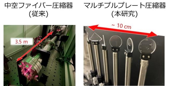 Fig. 2. 中空ファイバー圧縮器とマルチプレート圧縮器の写真。マルチプレート圧縮器は非常にコンパクト且つシンプルな構成であることがわかる。
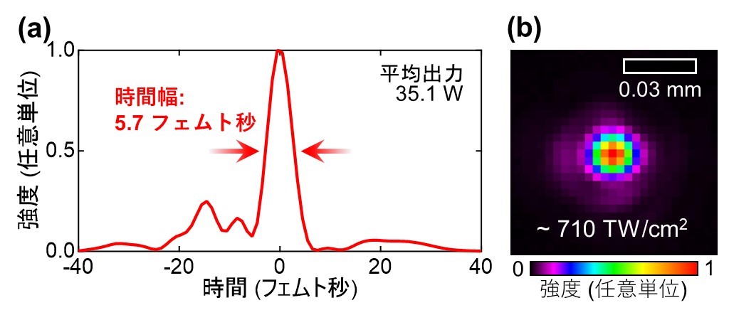 Fig. 3. (a) 1.7周期光パルスのパルス波形。(b) 集光した際のレーザーの様子。きれいな円形に集光できていることが分かる。
用語解説
- 繰り返しレート
一定の周期で発生するパルス光の1秒間にあたりのパルス発生数。例えば、1 秒間に 10個のパルスが発生する場合、繰り返しレートは10Hzである。
- マルチプルプレート法
透明な固体プレート(本研究はガラス)を適切な距離間隔で配置することでパルスを圧縮する方法。従来は気体を用いた圧縮法が用いられているが、固体は気体よりも原子が密に存在しているため応答が巨大であり、コンパクトなセットアップにできる利点を有する。
- 光パラメトリックチャープ増幅
弱いパルス光の時間幅を一旦引き延ばした後に光強度を増幅し、時間幅を短く戻すことで高強度な光パルスを発生させる手法。
- 高次高調波
高強度レーザー光を希ガス等の媒質に集光すると、そのレーザーの周波数の整数倍の周波数成分を持つ波長の短い光が発生する。特に、集光したレーザー光の周波数の数十倍といった高い次数に達する場合もあることから「高次高調波」と呼ばれている。
- アト秒パルス光
パルス幅がアト秒域(100京分の1秒、10-18秒)のパルス光。一般的には波長が100 nm以下の短い極端紫外光領域や軟X線領域の光であり、高次高調波によって発生される。アト秒レーザーをカメラのフラッシュのように使うことで、アト秒の時間スケールで高速で動く物理現象を観察できることから、人類が有する最も高速な技術であり、世界各国で盛んに研究されている。
- イッテルビウム(Yb)系増幅器
イッテルビウム(Yb)を添加したレーザー結晶を使用するレーザー増幅器。本研究ではタングステン酸カリウムガドリニウム結晶にYbが添加されたYb:KGW増幅器を使用した。特徴は発生効率が良いことから発熱が抑えられ、100 Wを超える高い出力で動作することができる点である。
- チタンサファイア増幅器
高強度のフェムト秒レーザー光を得るために古くから広く普及しているレーザー増幅器。サファイア結晶にチタンを添加したレーザー媒質を使用しており、短いパルス幅が得られるが、一方で繰り返しレートがkHz程度までしか動作できないという欠点がある。
- 中空ファイバー圧縮法
古くから広く用いられている気体ベースのパルス圧縮法。気体は光への応答性が比較的弱いことから、気体を封入した数mの長い中空ファイバーにレーザー光を導入することで、長距離相互作用させる手法。
- TW/cm2 (テラワット/センチメーター2乗)
1 cm × 1 cmの面積にどれほどのパワーが集中しているかの単位。TWは1012(1000億)を示すテラ(T)というSI接頭語がついたパワー(W、ワット)を現す。つまり1 TW/cm2は1 cm × 1 cmの面積に1000億ワットの光が集中していることを意味する。 一般的に100 TW/cm2を超えるパワーを物質に照射すると、原子核を周回している電子が引きはがされる。アト秒光はその引きはがした電子によって発生するため、100 TW/cm2を超える高強度レーザーがアト秒光発生には必須となる。
Flying electron spin control gates
https://doi.org/10.1038/s41467-022-32807-x
Paul L. J. Helgers1,3, J. A. H. Stotz1,2, H. Sanada3, Y. Kunihashi3, K. Biermann1, P. V. Santos1
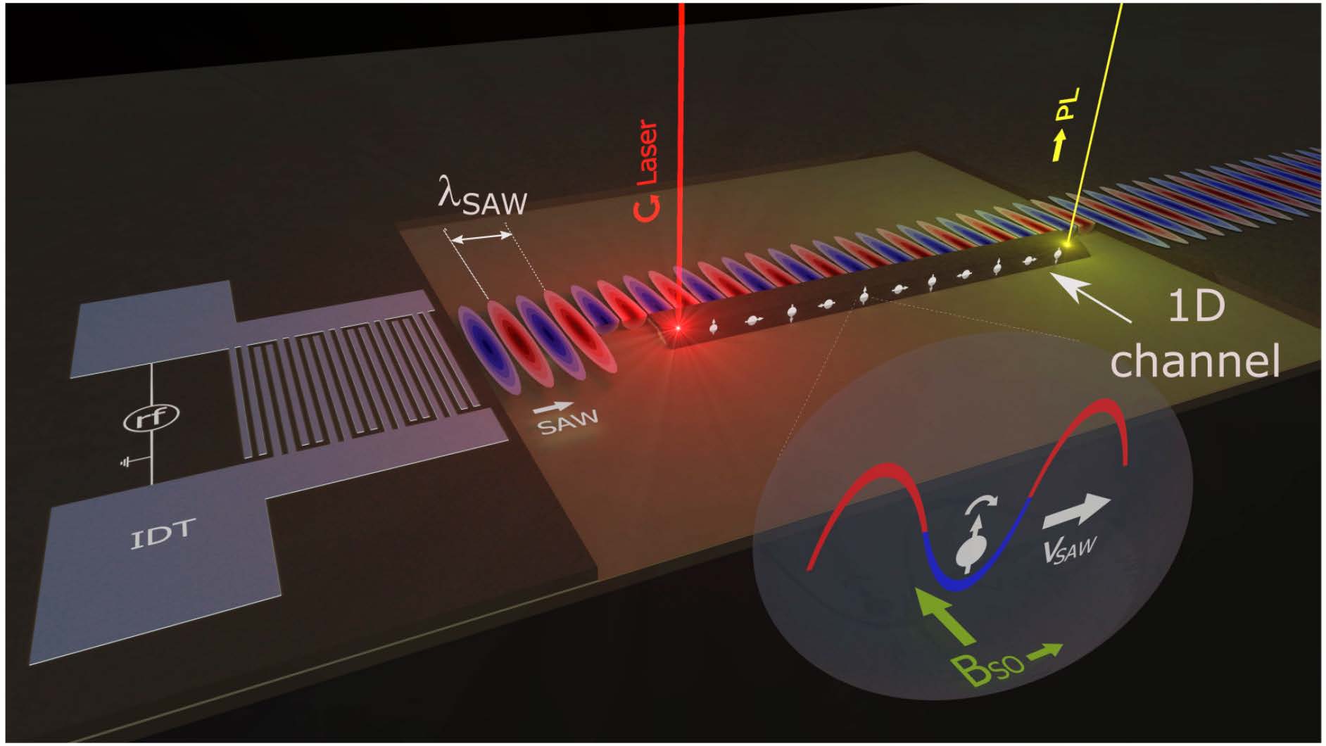 Fig. 1. Flying control gate for electron spins. A surface acoustic wave (SAW) excited by an interdigital acoustic transducer (IDT) aligned to a narrow semiconductor channel creates a train of dot-like moving potentials. Within the channel, a circularly polarized laser beam excites spin-polarized electrons and holes, which are captured by the moving dots and transport them with the SAW velocity, vSAW. Simultaneously, the SAW fields induce an effective magnetic field BSO that acts on the moving spins with a magnitude proportional to the SAW amplitude. By adjusting the SAW amplitude, the spin precession rate and be controlled yielding an electrically driven flying spin gate.
Electrons spins are attractive qubits for the implementation of quantum functionalities in semiconductor devices. In this context, the spin transitor proposed by Datta and Das [Datta and Das, Appl. Phys. Lett., 56, 665 (1990)] has been a guiding concept towards the implementation of spin-based functionalities in III-V semiconductor structures. The concept relies on the control of the spin vector of a moving (or flying) electron spin by an electrostatic field applied perpendicular to the motion. While eliminating the need for magnetic fields from spin devices is desirable, the most appealing feature of electrostatic spin control is compatibility with the field effect transitors widely used in semiconductor chips. Electrostatic spin control also requires, however, a precise control of the spin motion on the microscopic scale to avoid fluctuations in the spin orientation (spin decoherence). Consequently, Datta and Das spin transistors have, so far, only been demonstrated for ballistic spin transport along short (< 2 μm) channels [Koo et al., Science 325, 1515 (2009), Chuang et al., Nat. Nanotehnol. 10, 35 (2015)]. A major challenge for efficient spin control is to devise suitable approaches to both drive spin motion and, simultaneously, control the spin orientation while avoiding decoherence.
In a recent publication, Helgers et al. [Nat. Commun. 13, 5384 (2022)] have introduced an elegant solution for this challenge based on spin transport using moving potentials produced by a surface acoustic wave (SAW). SAWs are acoustic vibrations that travel along a surface in a manner analogous to earthquake waves. SAWs with micrometer-sized wavelengths can be electrically generated using interdigitated transducers (IDTs) fabricated on a semiconductor chip, as illustrated in Fig. 1. When applied along a narrow semiconductor channel, the SAW fields create moving potential dots, which capture the electrons and transport them with the acoustic velocity. The limited motion within the dots suppresses spin decoherence and enables electron spin transfer over distances up to 100 μm. [Stotz et al., Nat. Mat. 4, 585 (2005)]. Concomitantly with the transport, the SAW fields forming the dots and moving congruently with them can also manipulate the electron spin vector through spin precession. By changing the strength of the SAW, the precession rate will also be changed. As a result, the moving dots act as contactless, flying spin gates, which simultaneously drive the motion of the spins and dynamically control the rate of spin precession during transport.
Helgers et al. have now experimentally demonstrated the feasibility of this approach by controlling the spin precession rate using the SAW amplitude during transport. In the experiment, spin polarized electrons and holes were optically excited within the dots using a circularly polarized laser beam (cf. red beam in Fig. 1). These carriers were then acoustically transported over distances of up to 100 μm before they are forced to recombine emitting photons (green beam). From the analysis of the photon polarization, which reflects the spin state of the carriers prior to recombination, the authors determined the dependence of the spin vector on the transport distance, and the spins were observed to precess over many cycles during transport. More important, by electrically changing amplitude of the SAW field, the authors show that the precession rate can be change by over 200%, thus demonstrating an efficient flying gate for spin control.
The acoustically driven flying spin gates enable a high degree of dynamic spin control as well as on-chip spin transfer over several tens of micrometers by simply changing the amplitude of the carrier acoustic wave. The approach is compatible with planar technology and also offers a convenient interface for the interconversion between electron spins and polarized phonons for long-distance quantum information transfer. Furthermore, it can be extended for the control of single spin qubits by reducing the dot sizes to enclose single electron spins and, in this way, enable the generation on-demand of single photons with controlled polarization. The flying spin gates can thus act as a single spin qubit control gate, a key element for on-chip quantum information processing, with a photonic interface.
We acknowledge the financial support by the Natural Science and Engineering Research Council of Canada and the Alexander von Humboldt Foundation, Germany. This project has received funding from the European Union’s Horizon 2020 research and innovation program under grant agreement No 642688.
1 Paul-Drude-Institut für Festkörperelektronik, Leibniz-Institut im Forschungsverbund Berlin e.V., Hausvogteiplatz 5-7, 10117 Berlin, Germany
2 Department of Physics, Engineering Physics & Astronomy, Queen’s University, Kingston, ON, K7L3N6 Canada
3 NTT Basic Research Laboratories, NTT Corporation, 3-1 Morinosato-Wakamiya, Atsugi, Kanagawa 243-0198, Japan