


High-speed single-electron transfer toward high-accuracy current standards
- Transfer of electrons one by one via a charge trap in silicon transistors -
NTT Basic Research Laboratories have succeeded for the first time in speeding up one-by-one transfer of electrons via a charge-confining trap level*1 in silicon transistors*2.
Since a flow of electrons accurately transferred in one direction leads to a high-accuracy current flow, the technique is expected to lead to high-accuracy current sources (current standards*3), which will contribute to the recently proposed redefinition of the ampere (the base unit of electric current). In addition, if we realize a device with much higher accuracy than traditional electrical standards, we can contribute to the electrical standards field and the measurement instrument industry.
This work will be reported in the UK science journal "Nature Communications" on the 6th of October, 2014.
This work was partly supported by the Funding Program for Next Generation World-Leading Researchers of the Japan Society for the Promotion of Science (GR 103).
=> Press Release
=> Nanodevices Research Group
NTT Basic Research Laboratories have been developing single-electron devices that can manipulate and detect an individual electron, which is the smallest constituent of electric current. Such devices have attracted much interest for ultralow-power-consumption information processing and ultrahigh-sensitivity sensors because they can operate with a small number of charges and have a high charge sensitivity. We have so far demonstrated the operation of single-electron transfer devices and single-electron detectors using stable and reproducible silicon transistors.
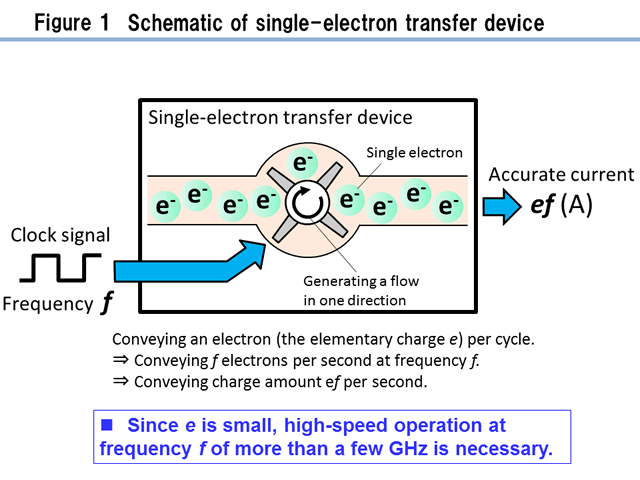
The redefinition of the ampere, the base unit of electric current defined in the International System of Units (SI)*4, was proposed in 2011 together with the abolition of the international prototype kilogram*5, and it has been attracting much attention. In the new SI units, the value of the elementary charge e, which has so far been determined from measurements, is fixed and the ampere is set from the fixed value. It is therefore desirable to realize the current standard using single-electron transfer because it directly connects e to the ampere (Figure 1).
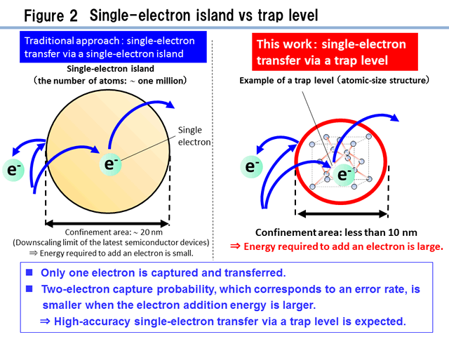
Most single-electron transfer devices control the transfer by capturing electrons in a single-electron island*6, an artificially fabricated fine region. To increase the transfer accuracy, we have to scale down the single-electron island to increase the energy (electron addition energy*7) required to capture an electron (Figure 2). However, the limitation on the downscaling of semiconductor devices has been an obstacle to increasing the transfer accuracy.
We have been studying single-electron manipulation to apply it to the electrical standards field, where high accuracy and reliability are required.
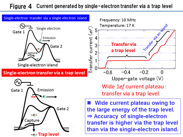
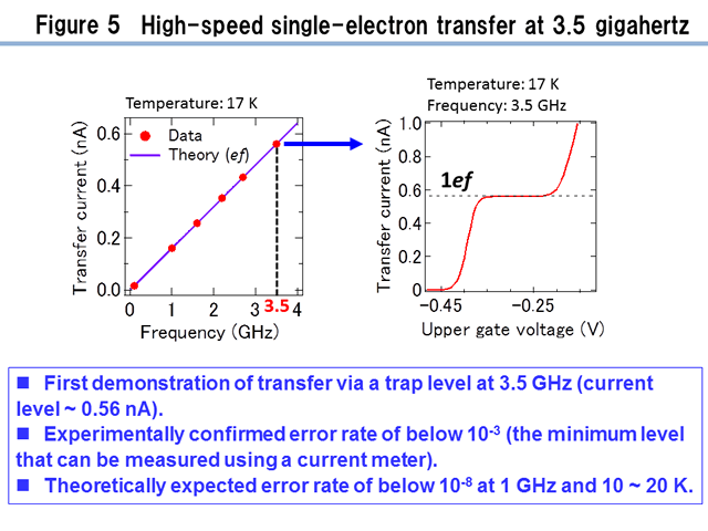
We have succeeded for the first time in high-speed single-electron transfer via a charge trap level in silicon transistors (Figure 3, Figure 4) at frequencies of up to 3.5 gigahertz and a measurement temperature of 17 kelvin*8 (Figure 5). In the high-speed operation, the error rate*9 is below the level that can be measured using a current meter (~ 10-3). The error rate obtained at 3.5 gigahertz is much lower than that of other single-electron transfer devices operating at a similar speed. In addition, from a theoretical estimation, the error rate is likely to be below 10-8 (the target for the current standards) at 10 to 20 K and 1 GHz, indicating the possibility of high-accuracy device operation.
Details of measurements and observation
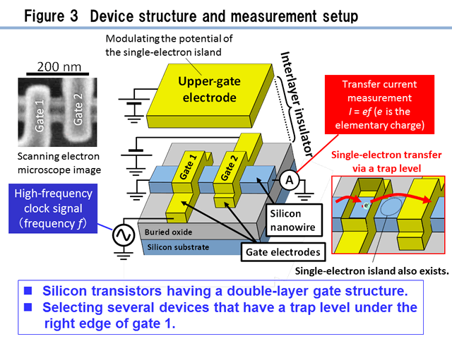
- Using silicon nanofabrication techniques, we fabricated a double-layer gate structure, in which two transistors with fine gate electrodes (gates 1 and 2) were formed on a silicon nanowire and an upper gate electrode was formed to cover the two gates and nanowire (Figure 3). When negative voltages are applied to gates 1 and 2, a single-electron island is electrically formed in the silicon nanowire between the two gates. The upper gate controls the potential of the single-electron island. From the fabricated devices, we selected several devices that have a trap level under the right edge of gate 1.
- A potential barrier is formed in the silicon nanowire under gate 2 by applying a negative voltage to it, and a high-frequency clock signal is applied to gate 1 (Figure 3, Figure 4). When the potential barrier in the silicon nanowire under gate 1 is sufficiently low (the value of the clock signal is positive), a single electron is captured by the trap level from the silicon nanowire on the left side of gate 1. After that, when the potential barrier in the silicon nanowire under gate 1 is sufficiently high (the value of the clock signal is negative), the captured single electron is emitted to the silicon nanowire on the right side of gate 2. The current flow resulting from the transfer of electrons from left to right was measured at 17 K.
- When the voltage applied to the upper gate is changed, we observe a wide current plateau*10 owing to the large electron addition energy of the trap level (Figure 4). With increasing voltage applied to the upper gate, current plateaus originating not only from the trap level but also from the single-electron island are observed. However, the current plateau originating from the single-electron island is narrower than that originating from the trap level. Since the transfer accuracy is worse when the plateau is narrower, the transfer via the trap level is more accurate than that via the single-electron island in this structure.
- With increasing frequency f of the clock signal, transfer current ef increases. The measured values of the 1ef current plateau agree well with the theoretical values at up to 3.5 GHz (Figure 5). Detailed measurements of the transfer current at 3.5 GHz revealed that the error rate is below the minimum level that can be measured using a current meter (~ 10-3).
Technical Features
- Silicon nanofabrication techniques and measurement techniques for silicon single-electron devices
Owing to our wafer-level fabrication techniques for nanometer-scale silicon transistors having a double-layer gate structure, many devices can be fabricated with high yield. As a result, optimal devices can be efficiently selected. In addition, our knowledge of the single-electron manipulation, which has been acquired from many studies of silicon single-electron devices, has enabled us to clarify the operating mechanism of the transfer via the trap level and thereby to achieve the high-speed operation. - Using a trap level and clarification of its transfer mechanism
Instead of the single-electron island, using a naturally existing trap level having an extremely fine confinement area of less than 10 nm, which is difficult to artificially fabricate, can lead to high-accuracy operation owing to its large electron addition energy (Figure 2). We investigated the electron capture/emission to/from the trap level in detail to clarify the mechanism of the transfer and found that the capture and emission speeds can be widely modulated by controlling applied voltages. On the basis of the findings, we achieved the high-speed operation by increasing speed of the capture and emission. In addition, by investigating temperature dependence of the transfer current, we theoretically anticipated the transfer error rates.
We aim to experimentally prove that the single-electron transfer has the high accuracy necessary for the current standards. Furthermore, we also aim to contribute to the electrical standards field and the measurement instrument industry by developing devices with accuracy that exceeds traditional electrical standards. In addition, since the findings in this work are applicable not only to trap levels but also to other localized states, we expect to be able to improve device yields by using intentionally introducible impurity levels. By using such a technique, high-yield current standards are expected to be accomplished. Furthermore, in the long term, we aim to achieve ultralow-power-consumption devices based on single-electron manipulation and thereby contribute to the realization of a low-energy society.
Publication information
G. Yamahata, K. Nishiguchi, A. Fujiwara
"Gigahertz single-trap electron pumps in Si"
Nature Communications (2014).
Glossary
*1 ... Trap level
This is a naturally formed energy state that can capture an electric charge. Examples of traps originating from atomic-size structures are interface traps between silicon and silicon dioxide and crystal defects in silicon.
*2 ... Silicon transistors
These are devices fabricated using semiconducting silicon, which can switch or amplify electrical signals. In this work, we used field-effect transistors, in which electric current flowing in silicon is turned on or off by applying a voltage to a gate electrode. The gate electrode is formed on silicon via an insulator consisting of silicon dioxide.
*3 ... Current standards
These are standards for the base unit of electric current (the ampere). The ampere is now defined by a force produced by the same current flowing through two infinite-length conductors in a vacuum. However, since it is difficult to exactly achieve the conditions described in the definition in actual experiments, it has been suggested in the redefinition of the SI base units that the ampere be set by fixing the elementary charge e.
*4 ... The International System of Units (SI)
These are internationally adopted units, in which seven base units - time [the second (s)], length [the meter (m)], mass [the kilogram (kg)], electric current [the ampere (A)], thermodynamic temperature [the kelvin (K)], amount of substance [the mole (mol)], and luminous intensity [the candela (cd)] - are defined. Other units are derived from these base units. In the proposed redefinition of the SI units, instead of defining the base unit, fundamental physical constants are fixed and the base units are set from the constants.
*5 ... The international prototype kilogram
This is an alloy of platinum and iridium, which is now used as the definition of mass. The abolition of the international prototype kilogram has attracted much attention in the redefinition of the International System of Units (SI). Since the change in the weight of the international prototype kilogram due to surface contamination is a problem, it is desirable to universally define the mass to achieve long-term stability. In the new definition, the kilogram is set from the fixed Planck constant.
*6 ... Single-electron island
This is a fine island, in which the electron addition energy is sufficiently larger than the energy fluctuation originating from heat and thereby the constant number of electrons can be accumulated. The number of accumulated electrons can be controlled by externally applying voltage.
*7 ... Electron addition energy
This is the energy required to add one electron to a certain region. The value is mainly determined by the charging energy originating from electrostatic repulsion of electrons and the quantum-mechanical energy originating from confinement of electrons. The electron addition energy increases with the decreasing size of the region.
*8 ... Kelvin
This is the unit (K) of temperature. 0℃ corresponds to 273.15 K.
*9 ... Error rate
To be precise, this is the relative error rate, which is transfer-error probability when a single electron is transferred. For example, an error rate of 10-3 means that an average of one error occurs during a thousand transfers.
*10 ... Current plateau
This is a region where current levels are almost constant when a voltage is changed.


