


Successful Amplification of Transistor Current Without Additional Power
―On the path toward new low-power devices―
The research group of Professor Yukinori Ono of the Research Institute of Electronics (Director: Hidenori Mimura) and Graduate School of Science and Technology (Dean: Kazuhiko Hara), Shizuoka University (President: Kiyoshi Ishii) and others has successfully amplified transistor*1 current without additional power in collaboration with the research group of Akira Fujiwara, Senior Distinguished Researcher of Nippon Telegraph and Telephone Corporation (NTT, President & CEO: Jun Sawada) and Professor Yasuo Takahashi of Hokkaido University (President: Toyoharu Nawa).
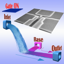
This method of current amplification applies the principle of an aspirator*2 that ejects water or air from a nozzle at high pressure. It therefore requires no additional power in contrast to traditional methods of amplification, which is a feature that should lead to the development of new devices with low power consumption. This result was announced on the online version of the British science journal “Nature Communications” on December 17th (United Kingdom time) under the title “Electron aspirator using electron–electron scattering in nanoscale silicon.”
=> Press Release
=> Nanodevices Research Group
Research background
Raising the performance of computers that provide the infrastructure of today’s information society depends on the degree to which current in transistors—the constituent elements of computers—can be increased with a small amount of electric power. However, amplification methods to date have required an additional supply of power, which is a factor in the generation of heat. As a result, this requirement has become a fundamental problem hindering improvements in computer performance.
Research results
A joint research team working with the Research Institute of Electronics and Graduate School of Science and Technology, Shizuoka University has successfully amplified transistor input current without supplying additional power at a temperature of 8 K (Kelvin; 8 K = -265.15°C) by applying the principle of an aspirator to a transistor device. It was experimentally shown that a new electron flow could be generated by using the energy that is usually consumed as heat in a flow of electrons. This should make it possible to suppress the generation of heat accompanying current amplification, which has so far been difficult to do.
Experiment overview
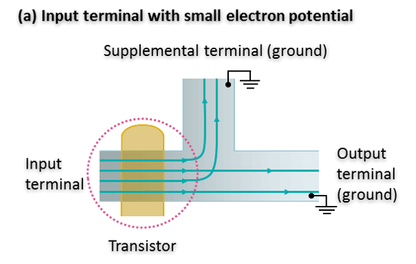
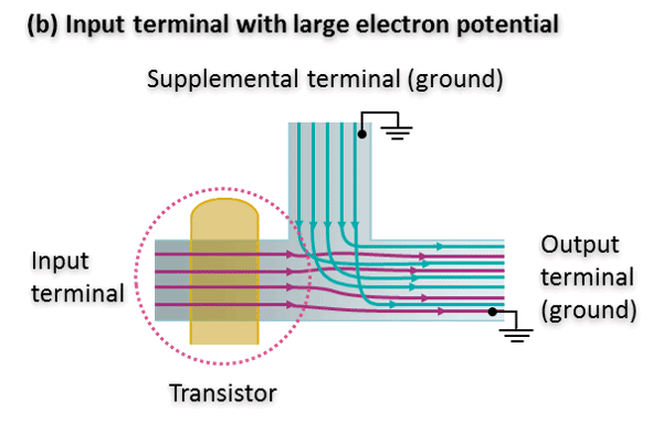
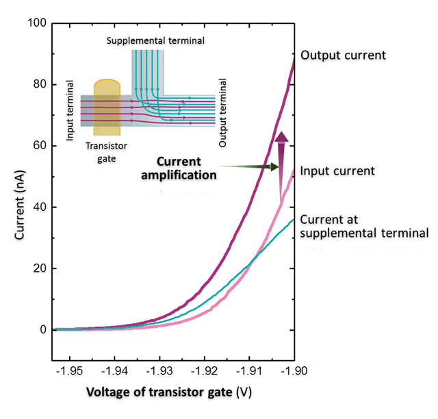
On a silicon substrate, we fabricated a structure that adds a supplemental terminal for introducing current via a side channel to the transistor’s output terminal. We then used this structure to measure current at the output terminal in a state in which both the output terminal and the supplemental terminal are grounded. When electron potential*3 at the input terminal for injecting electrons was small, the current was found to flow into the output terminal and to branch into the supplemental terminal as usually observed (Fig. 1 (a)). However, when making the electron potential large, a reverse flow of electrons (Fig. 1 (b)) was observed resulting in current amplification at the output terminal (Fig. 2).
Technical points: Observation of “electron fluid” on nanometer scale and its application
Electrons in matter usually move from a point of high potential to one of low potential, which means no electron flow between terminals of equal potential and no current flow as a result. However, in the special case that the frequency of electron-electron collisions is extremely high, electrons will behave in the manner of a fluid like water, so if a strong flow should exist nearby, a new flow will arise aligned with that flow. This type of electron behavior is called an electron fluid*4, but it had so far been observed only on a large scale of a micrometer or greater in some materials such as gallium arsenide (GaAs).
In the research reported here, we achieved an electron fluid in a transistor on a nanometer*5 scale by using an intense electric field generated within finely structured silicon and succeeded in generating a current flowing from a grounded supplemental terminal at potential zero. We also fabricated an “electron-aspirator” device using this phenomenon and demonstrated its current-amplification effect.
Future plans
The experiment described here used a device on a 90-nanometer scale and was therefore conducted at a low temperature of 8 K, but improvements in operating temperature can be expected with further downscaling. Our aim is to demonstrate operation of this device at room temperature with an eye to practical use.
Paper publication information:
H. Firdaus, T. Watanabe, M. Hori, D. Moraru, Y. Takahashi, A. Fujiwara and Y. Ono,
“Electron aspirator using electron-electron scattering in nanoscale silicon”
Nature Communications (2018).
Terminology
*1 ... Transistor
A semiconductor device that can switch or amplify electrical signals. The experiment presented here targeted a field effect transistor (a type of transistor that turns a current flowing in silicon ON/OFF by applying a voltage to the gate electrode formed on the silicon substrate via an insulating film), which is a major component of modern computers.
*2 ... Aspirator
A T-shaped tube having a suction port in addition to an inlet and outlet. Connecting the inlet to a water faucet and the outlet to a drain and letting a powerful stream of water flow from the faucet enables a liquid or gas to be drawn in from the suction port and to flow toward the drain. Since no electric power is needed for this operation, it can be easily used, for example, for the pumping of liquid or gas in chemical experiments. Also called a “jet pump.”
*3 ... Potential
The product of charge and voltage. Corresponds to energy. Since electron charge is negative, applying a negative voltage increases electron potential (energy). The potential of a grounded terminal is zero.
*4 ... Electron fluid
Indicates a state in which electrons behave like a fluid such as water. It can show unique characteristics not normally observed such as a negative electrical resistance caused by a vortex effect. It can be seen in special cases in which the frequency of electron-electron collisions is higher than the frequency of collisions with base semiconductor atoms (lattice) or impurities.
*5 ... Nanometer
10-9 meter or one thousand-millionth of a meter. Current cutting-edge transistors are being scaled down to a feature size of about 20 nanometers.


