Press Release

Publications in 2023

  1. M. Takiguchi, G. Q. Zhang, S. Sasaki, K. Tateno, C. John, M. Ono, H. Sumikura, A. Shinya, and M. Notomi

    Damage protection from focused ion beam process toward nanocavity-implemented compound semiconductor nanowire lasers

    Nanotechnology 34 (13), 135301 (2023).

  2. M. Kurosu, D. Hatanaka, R. Ohta, H. Yamaguchi, Y. Taniyasu, and H. Okamoto

    Impedance-matched high-overtone bulk acoustic resonator

    Appl. Phys. Lett. 122 (12), 122201 (2023).

Publications in 2022

  1. W. Tomita, S. Sasaki, M. Asano, K. Tateno, H. Okamoto, and H. Yamaguchi

    Double-Gate Vectorial Frequency Control in Piezoresistive Nanowire Electromechanical Devices

    Phys. Rev. Appl. 17 (4), 044042 (2022).

  2. M. Kawano, K. Hirama, and K. Kumakura

    High blocking temperature of Fe nanoparticles embedded in diamond thin films

    AIP Adv. 12 (4), 045022 (2022).

  3. M. Hiroki, Y. Taniyasu, and K. Kumakura

    High-Temperature Performance of AlN MESFETs With Epitaxially Grown n-Type AlN Channel Layers

    IEEE Electron Device Lett. 43 (3) 350-353 (2022).

Publications in 2021

  1. K. Takase, K. Tateno, and S. Sasaki

    Electrical tuning of the spin-orbit interaction in nanowire by transparent ZnO gate grown by atomic layer deposition

    Appl. Phys. Lett. 119 (1), 013102 (2021).

Publications in 2020

  1. M. Takiguchi, S. Sasaki, K. Tateno, E. Chen, K. Nozaki, S. Sergent, E. Kuramochi, G. Q. Zhang, A. Shinya, and M. Notomi

    Hybrid Nanowire Photodetector Integrated in a Silicon Photonic Crystal

    ACS Photonics 7 (12) 5467-5473 (2020).

  2. N. Kumada, N. H. Tu, K. Sasaki, T. Ota, M. Hashisaka, S. Sasaki, K. Onomitsu, and K. Muraki

    Suppression of gate screening on edge magnetoplasmons by highly resistive ZnO gate

    Phys. Rev. B 101 (20), 205205 (2020).

  3. K. Hirama, Y. Taniyasu, H. Yamamoto, and K. Kumakura

    Control of n-type electrical conductivity for cubic boron nitride (c-BN) epitaxial layers by Si doping

    Appl. Phys. Lett. 116 (16)(2020).

  4. M. Takiguchi, N. Takemura, K. Tateno, K. Nozaki, S. Sasaki, S. Sergent, E. Kuramochi, T. Wasawo, A. Yokoo, A. Shinya, and M. Notomi

    All-Optical InAsP/InP Nanowire Switches Integrated in a Si Photonic Crystal

    ACS Photonics 7 (4) 1016-1021 (2020).

  5. H. Sumikura, K. Hirama, K. Nishiguchi, A. Shinya, and M. Notomi

    Highly nitrogen-vacancy doped diamond nanostructures fabricated by ion implantation and optimum annealing

    APL Mater. 8 (3), 031113 (2020).

  6. H. Irie, T. Akiho, F. Couedo, R. Ohana, K. Suzuki, K. Onomitsu, and K. Muraki

    Impact of epitaxial strain on the topological-nontopological phase diagram and semimetallic behavior of InAs/GaSb composite quantum wells

    Phys. Rev. B 101 (7), 075433 (2020).

  7. H. Sanada, A. M. Stramma, Y. Kunihashi, Y. Tanaka, H. Gotoh, K. Onomitsu, F. Tagarelli, M. Kohda, J. Nitta, and T. Sogawa

    Spin accumulation in photo-induced potential dimples generated in semiconductors

    Commun. Phys. 3 (1), 11 (2020).

Publications in 2019

  1. K. Suzuki, K. Onomitsu, and K. Kanisawa

    Tunneling spectroscopy of an indium adatom precisely manipulated on the cross-sectional surface of InAs/GaSb quantum structures

    Phys. Rev. B 100 (23), 235306 (2019).

  2. W. Tomita, S. Sasaki, K. Tateno, H. Okamoto, and H. Yamaguchi

    Novel Fabrication Technique of Suspended Nanowire Devices for Nanomechanical Applications

    Phys. Status Solidi B-Basic Solid State Phys. , 1900401 (2019).

  3. M. Hiroki, and K. Kumakura

    Ohmic contact to AlN:Si using graded AlGaN contact layer

    Appl. Phys. Lett. 115 (19), 192104 (2019).

  4. H. Okamoto, K. Takita, K. Tsushima, T. Tawara, K. Tateno, G. Q. Zhang, and H. Gotoh

    Low-temperature formation of GeSn nanodots by Sn mediation

    Jpn. J. Appl. Phys. 58, SDDG09 (2019).

  5. K. Tsushima, K. Takita, H. Nakazawa, T. Tawara, K. Tateno, G. Q. Zhang, H. Gotoh, and H. Okamoto

    Study on the formation mechanism of bismuth-mediated Ge nanodots fabricated by vacuum evaporation

    Jpn. J. Appl. Phys. 58, SDDG10 (2019).

  6. M. Takamura, N. Kumada, S. N. Wang, K. Kumakura, and Y. Taniyasu

    Plasmon Control Driven by Spatial Carrier Density Modulation in Graphene

    ACS Photonics 6 (4) 947-952 (2019).

  7. K. Hirama, Y. Taniyasu, H. Yamamoto, and K. Kumakura

    Structural analysis of cubic boron nitride (111) films heteroepitaxially grown on diamond (111) substrates

    J. Appl. Phys. 125 (11), 115303 (2019).

  8. G. Q. Zhang, M. Takiguchi, K. Tateno, T. Tawara, M. Notomi, and H. Gotoh

    Telecom-band lasing in single InP/InAs heterostructure nanowires at room temperature

    Sci. Adv. 5 (2), eaat8896 (2019).

  9. Y. Tanaka, Y. Kunihashi, H. Sanada, H. Gotoh, K. Onomitsu, M. Kohda, J. Nitta, and T. Sogawa

    Phase velocity of drifting spin wave packets in semiconductor two-dimensional electron gas

    Appl. Phys. Express 12 (1), 013001 (2019).

  10. K. Tateno, G. Q. Zhang, S. Sasaki, M. Takiguchi, and K. Kumakura

    Wurtzite GaP nanowire grown by using tertiarybutylchloride and used to fabricate solar cell

    Jpn. J. Appl. Phys. 58 (1), 015004 (2019).

Publications in 2018

  1. K. Tateno, G. Q. Zhang, M. Takiguchi, and H. Gotoh

    Alternating InAsP/InP heterostructure nanowires grown with tertiary-butyl chloride

    Nano Futures 2 (4), UNSP 045006 (2018).

  2. K. Suzuki, and T. Akasaka

    Landau level quantization with gate tuning in an AlN/GaN single heterostructure

    Jpn. J. Appl. Phys. 57 (11), 111001 (2018).

  3. T. Akasaka, M. Schied, and K. Kumakura

    N-face (0001) GaN/InN/GaN double heterostructures emitting near-infrared photoluminescence grown by metalorganic vapor phase epitaxy

    Appl. Phys. Express 11 (8), 081001 (2018).

  4. M. Takiguchi, G. Q. Zhang, S. Sasaki, K. Nozaki, E. Chen, K. Tateno, T. Tawara, A. Shinya, H. Gotoh, and M. Notomi

    Direct modulation of a single InP/InAs nanowire light-emitting diode

    Appl. Phys. Lett. 112 (25), 251106 (2018).

  5. S. Norimoto, S. Nakamura, Y. Okazaki, T. Arakawa, K. Asano, K. Onomitsu, K. Kobayashi, and N. H. Kaneko

    Fano effect in the transport of an artificial molecule

    Phys. Rev. B 97 (19), 195313 (2018).

  6. M. Kurosu, D. Hatanaka, K. Onomitsu, and H. Yamaguchi

    On-chip temporal focusing of elastic waves in a phononic crystal waveguide

    Nat. Commun. 9, 1331 (2018).

  7. K. Ebata, J. Nishinaka, Y. Taniyasu, and K. Kumakura

    High hole concentration in Mg-doped AlN/AlGaN superlattices with high Al content

    Jpn. J. Appl. Phys. 57 (4), 04FH09 (2018).

  8. G. Q. Zhang, K. Tateno, T. Sogawa, and H. Gotoh

    Diameter-tailored telecom-band luminescence in InP/InAs heterostructure nanowires grown on InP (111)B substrate with continuously-modulated diameter from microscale to nanoscale

    Nanotechnology 29 (15), 155202 (2018).

  9. T. Hayashi, A. Naka, M. Hiroki, T. Yokota, T. Someya, and A. Fujiwara

    Transport characteristics in Au/pentacene/Au diodes

    Jpn. J. Appl. Phys. 57 (3), 03EH07 (2018).

  10. Y. Okazaki, S. Nakamura, K. Onomitsu, and N. H. Kaneko

    Digital processing with single electrons for arbitrary waveform generation of current

    Appl. Phys. Express 11 (3), 036701 (2018).

Publications in 2017

  1. D. Hatanaka, T. Darras, I. Mahboob, K. Onomitsu, and H. Yamaguchi

    Broadband reconfigurable logic gates in phonon waveguides

    Sci Rep 7, 12745 (2017).

  2. S. Suzuki, Y. Sekine, and K. Kumakura

    Terahertz spectroscopy of graphene complementary split ring resonators with gate tunability

    Jpn. J. Appl. Phys. 56 (9), 095102 (2017).

  3. M. Hiroki, K. Kumakura, and H. Yamamoto

    Efficient heat dissipation in AlGaN/GaN high electron mobility transistors by substrate-transfer technique

    Phys. Status Solidi A-Appl. Mat. 214 (8), UNSP 1600845 (2017).

  4. T. Akasaka, C. H. Lin, H. Yamamoto, and K. Kumakura

    Surface supersaturation in flow-rate modulation epitaxy of GaN

    J. Cryst. Growth 468 821-826 (2017).

  5. K. Takase, Y. Ashikawa, G. Zhang, K. Tateno, and S. Sasaki

    Highly gate-tuneable Rashba spin-orbit interaction in a gate-all-around InAs nanowire metal-oxide-semiconductor field-effect transistor

    Sci Rep 7, 930 (2017).

  6. A. Yokoo, M. Takiguchi, M. D. Birowosuto, K. Tateno, G. Q. Zhang, E. Kuramochi, A. Shinya, H. Taniyama, and M. Notomi

    Subwavelength Nanowire Lasers on a Silicon Photonic Crystal Operating at Telecom Wavelengths

    ACS Photonics 4 (2) 355-362 (2017).

  7. K. Hirama, Y. Taniyasu, S. I. Karimoto, H. Yamamoto, and K. Kumakura

    Heteroepitaxial growth of single-domain cubic boron nitride films by ion-beam-assisted MBE

    Appl. Phys. Express 10 (3), 035501 (2017).

  8. J. Nishinaka, Y. Taniyasu, T. Akasaka, and K. Kumakura

    Surface morphology control of nonpolar m-plane AlN homoepitaxial layers by flow-rate modulation epitaxy

    Phys. Status Solidi B-Basic Solid State Phys. 254 (2), 1600545 (2017).

Publications in 2016

  1. C.-H. Lin, T. Akasaka, and H. Yamamoto

    N-face GaN(0001) films with hillock-free smooth surfaces grown by group-III-source flow-rate modulation epitaxy

    Jpn. J. Appl. Phys. 55, 04EJ01 (2016).

  2. M. Kasu, K. Hirama, K. Harada, and T. Oishi

    Study on capacitance?voltage characteristics of diamond field-effect transistors with NO2 hole doping and Al2O3 gate insulator layer

    Jpn. J. Appl. Phys. 55, 041301 (2016)..

  3. M. Hiroki, K. Kumakura, and H. Yamamoto

    Enhancement of performance of AlGaN/GaN high-electron-mobility transistors by transfer from sapphire to a copper plate

    Jpn. J. Appl. Phys. 55, 05FH07 (2016). .

  4. J. Nishinaka, M. Funato, R. Kido, and Y. Kawakami

    InGaN/AlGaN stress compensated superlattices coherently grown on semipolar (1122) GaN substrates

    Phys. Status Solidi B-Basic Solid State Phys. 253 (1) 78-83 (2016).

Publications in 2015

  1. T. Makimoto, K. Kumakura, M. Maeda, H. Yamamoto and Y. Horikoshi

    A new AlON buffer layer for RF-MBE growth of AlN on a sapphire substrate

    J. Cryst. Growth 425, 138-140 (2015).

  2. M. Naito, K. Uehara, R. Takeda, Y. Taniyasu and H. Yamamoto

    Growth of iron nitride thin films by molecular beam epitaxy

    J. Cryst. Growth 415, 36-40 (2015).

  3. S. Sasaki, K. Tateno, G. Q. Zhang, H. Pigot, Y. Harada, S. Saito, A. Fujiwara, T. Sogawa and K. Muraki

    Self-aligned gate-all-around InAs/InP core-shell nanowire field-effect transistors

    Jpn. J. Appl. Phys. 54, 04DN04 (2015).

Publications in 2014

  1. T. Akasaka and H. Yamamoto

    Nucleus and spiral growth mechanisms of nitride semiconductors in metalorganic vapor phase epitaxy

    Jpn. J. Appl. Phys. 53 (10), 100201 (2014).

  2. R. G. Banal, Y. Taniyasu and H. Yamamoto

    Deep-ultraviolet light emission properties of nonpolar M-plane AlGaN quantum wells

    Appl. Phys. Lett. 105 (5), 053104 (2014).

  3. Chia-Hung Lin, T. Akasaka and H. Yamamoto

    N-face GaN(0001) films grown by group-III-source flow-rate modulation epitaxy

    Jpn. J. Appl. Phys. 53 (11S), 11RC01 (2014).

  4. J. Dai, R. Kometani, K. Onomitsu, Y. Krockenberger, H. Yamaguchi, S. Ishihara and S. Warisawa

    Direct fabrication of a W-C SNS Josephson junction using focused-ion-beam chemical vapour deposition

    J. Micromech. Microeng. 24 (5), 055015 (2014).

  5. K. Hirama, Y. Taniyasu, S. Karimoto, Y. Krockenberger and H. Yamamoto

    Single-crystal cubic boron nitride thin films grown by ion-beam-assisted molecular beam epitaxy

    Appl. Phys. Lett. 104 (9), 092113 (2014).

  6. M. Hiroki, K. Kumakura, Y. Kobayashi, T. Akasaka, T. Makimoto and H. Yamamoto

    Suppression of self-heating effect in AlGaN/GaN high electron mobility transistors by substrate-transfer technology using h-BN

    Appl. Phys. Lett. 105 (19), 193509 (2014).

  7. K. M. Kojima, Y. Krockenberger, I. Yamauchi, M. Miyazaki, M. Hiraishi, A. Koda, R. Kadono, R. Kumai, H. Yamamoto, A. Ikeda and M. Naito

    Bulk superconductivity in undoped T '-La1.9Y0.1CuO4 probed by muon spin rotation

    Phys. Rev. B 89 (18), 180508 (2014).

  8. Y. Krockenberger, B. Eleazer, H. Irie and H. Yamamoto

    Superconducting- and Insulating-Ground States in La2CuO4 Structural Isomers

    J. Phys. Soc. Jpn. 83 (11), 114602 (2014).

  9. Y. Krockenberger, H. Irie, J. Yan, L. Waterston, B. Eleazer, K. Sakuma and H. Yamamoto

    Superconductivity in cuprates with square-planar coordinated copper driven by hole carriers

    Appl. Phys. Express 7 (6), 063101 (2014).

  10. K. Takahashi, M. Imamura, K. Hirama and M. Kasu

    Electronic states of NO2-exposed H-terminated diamond/Al2O3 heterointerface studied by synchrotron radiation photoemission and X-ray absorption spectroscopy

    Appl. Phys. Lett. 104 (7), 072101 (2014).

  11. C. H. Lin, T. Akasaka, and H. Yamamoto

    N-face GaN(0001) films grown by group-III-source flow-rate modulation epitaxy

    Jpn. J. Appl. Phys. 53 (11), 11RC01 (2014).

Publications in 2013

  1. T. Akasaka, Y. Kobayashi, M. Kasuy, and H. Yamamoto

    Carrier Gas Dependent Evaporation Energy of GaN Estimated from Spiral Growth Rates in Selective-Area Metalorganic Vapor Phase Epitaxy

    Appl. Phys. Express 6 (10), 105501 (2013).

  2. J. Dai, K. Onomitsu, R. Kometani, Y. Krockenberger, H. Yamaguchi, S. Ishihara, and S. Warisawa

    Superconductivity in Tungsten-Carbide Nanowires Deposited from the Mixtures of W(CO)6 and C14H10

    Jpn. J. Appl. Phys. 52 (7), (2013).

  3. M. Hiroki, Y. Oda, N. Watanabe, N. Maeda, H. Yokoyama, K. Kumakura, and H. Yamamoto

    Unintentional Ga incorporation in metalorganic vapor phase epitaxy of In-containing III-nitride semiconductors

    J. Cryst. Growth 382, 36-40 (2013).

  4. M. Hiroki, N. Watanabe, N. Maeda, H. Yokoyama, K. Kumakura, and H. Yamamoto

    Influence of Metalorganic Vapor Phase Epitaxy Regrowth on Characteristics of InAlN/AlGaN/GaN High Electron Mobility Transistors

    Jpn. J. Appl. Phys. 52 (4), (2013).

  5. Y. Krockenberger, H. Irie, O. Matsumoto, K. Yamagami, M. Mitsuhashi, A. Tsukada, M. Naito, and H. Yamamoto

    Emerging superconductivity hidden beneath charge-transfer insulators

    Sci Rep 3, 2235 (2013).

  6. CH. Lin, T. Akasaka, and H. Yamamoto

    Nucleus and Spiral Growth of N-face GaN(0001) Obtained by Selective-Area Metalorganic Vapor Phase Epitaxy

    Appl. Phys. Express 6 (3), 035503 (2013).

  7. J. Nishinaga, A. Kawaharazuka, K. Onomitsu, and Y. Horikoshi

    High-Absorption-Efficiency Superlattice Solar Cells by Excitons

    Jpn. J. Appl. Phys. 52 (11), (2013).

  8. H. Sato, and M. Kasu

    Maximum hole concentration for Hydrogen-terminated diamond surfaces with various surface orientations obtained by exposure to highly concentrated NO2

    Diam. Relat. Mat. 31, 47-49 (2013).

  9. Y. Takagi, K. Shiraishi, M. Kasu, and H. Sato

    Mechanism of hole doping into hydrogen terminated diamond by the adsorption of inorganic molecule

    Surf. Sci. 609, 203-206 (2013).

  10. H. Yamamoto, Y. Krockenberger, and M. Naito

    Multi-source MBE with high-precision rate control system as a synthesis method sui generis for multi-cation metal oxides

    J. Cryst. Growth 378, 184-188 (2013).

  11. N. Maeda, M. Hiroki, S. Sasaki, and Y. Harada

    High-Temperature Characteristics in Recessed-Gate AlGaN/GaN Enhancement-Mode Heterostructure Field Effect Transistors with Enhanced-Barrier Structures

    Jpn. J. Appl. Phys. 52 (8), (2013).

  12. K. Suzuki, Y. Harada, K. Onomitsu, and K. Muraki

    Edge channel transport in the InAs/GaSb topological insulating phase

    Phys. Rev. B 87 (23), 235311 (2013).

  13. H. Sanada, Y. Kunihashi, H. Gotoh, K. Onomitsu, M. Kohda, J. Nitta, PV. Santos, and T. Sogawa

    Manipulation of mobile spin coherence using magnetic-field-free electron spin resonance

    Nat. Phys. 9 (5), 280-283 (2013).

Publications in 2012

  1. T. Akasaka, H. Gotoh, Y. Kobayashi, and H. Yamamoto

    Extremely Narrow Violet Photoluminescence Line from Ultrathin InN Single Quantum Well on Step-Free GaN Surface

    Advanced Materials 24 (31), 4296+ (2012).

  2. K. Hirama, M. Kasu, and Y. Taniyasu

    RF High-Power Operation of AlGaN/GaN HEMTs Epitaxially Grown on Diamond

    Ieee Electron Device Letters 33 (4), 513515 (2012).

  3. K. Hirama, M. Kasu, and Y. Taniyasu

    Growth and Device Properties of AlGaN/GaN High-Electron Mobility Transistors on a Diamond Substrate

    Japanese Journal Of Applied Physics 51 (1), 01AG09 (2012).

  4. K. Hirama, H. Sato, Y. Harada, H. Yamamoto, and M. Kasu

    Thermally Stable Operation of H-Terminated Diamond FETs by NO2 Adsorption and Al2O3 Passivation

    Ieee Electron Device Letters 33 (8), 11111113 (2012).

  5. K. Hirama, H. Sato, Y. Harada, H. Yamamoto, and M. Kasu

    Diamond Field-Effect Transistors with 1.3A/mm Drain Current Density by Al2O3 Passivation Layer

    Japanese Journal Of Applied Physics 51 (9), 090112 (2012).

  6. K. Hirama, Y. Taniyasu, and M. Kasu

    Epitaxial Growth of AlGaN/GaN High-Electron Mobility Transistor Structure on Diamond (111) Surface

    Japanese Journal Of Applied Physics 51 (9), 090114 (2012).

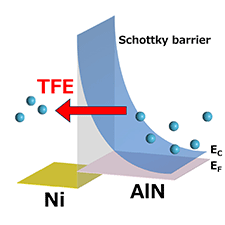
  7. K. Kamiya, Y. Ebihara, M. Kasu, and K. Shiraishi

    Efficient Structure for Deep-Ultraviolet Light-Emitting Diodes with High Emission Efficiency: A First-Principles Study of AlN/GaN Superlattice

    Japanese Journal Of Applied Physics 51 (2), 02BJ11 (2012).

  8. M. Kasu, H. Sato, and K. Hirama

    Thermal Stabilization of Hole Channel on H-Terminated Diamond Surface by Using Atomic-Layer-Deposited Al2O3 Overlayer and its Electric Properties

    Applied Physics Express 5 (2), 025701 (2012).

  9. Y. Kobayashi, K. Kumakura, T. Akasaka, and T. Makimoto

    Layered boron nitride as a release layer for mechanical transfer of GaN-based devices

    Nature 484 (7393), 223227 (2012).

  10. Y. Krockenberger, K. Sakuma, and H. Yamamoto

    Molecular Beam Epitaxy and Transport Properties of Infinite-Layer Sr0.90La0.10CuO2 Thin Films

    Applied Physics Express 5 (4), 043101 (2012).

  11. Y. Krockenberger, H. Yamamoto, M. Mitsuhashi, and M. Naito

    Universal Superconducting Ground State in Nd1.85Ce0.15CuO4 and Nd2CuO4

    Japanese Journal Of Applied Physics 51 (1), 010106 (2012).

  12. Y. Krockenberger, H. Yamamoto, A. Tsukada, M. Mitsuhashi, and M. Naito

    Unconventional transport and superconducting properties in electron-doped cuprates

    Physical Review B 85 (18), 184502 (2012).

  13. T. Makimoto, K. Kumakura, Y. Kobayashi, T. Akasaka, and H. Yamamoto

    A Vertical InGaN/GaN Light-Emitting Diode Fabricated on a Flexible Substrate by a Mechanical Transfer Method Using BN

    Applied Physics Express 5 (7), 072102 (2012).

  14. H. Sato, and M. Kasu

    Electronic properties of H-terminated diamond during NO2 and O3 adsorption and desorption

    Diamond And Related Materials 24 (), 99103 (2012).

  15. Y. Taniyasu, JF. Carlin, A. Castiglia, R. Butte, and N. Grandjean

    Mg doping for p-type AlInN lattice-matched to GaN

    Applied Physics Letters 101 (8), 082113 (2012).

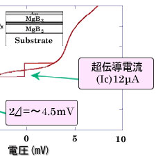
  16. Y. Krockenberger, S. Karimoto, H. Yamamoto, and K. Semba

    Coherent growth of superconducting TiN thin films by plasma enhanced molecular beam epitaxy

    Journal Of Applied Physics 112 (8), 083920 (2012).