
|
|
 |
 |
 |
 |
 |
 |
 Home
Home |
People |
Publications |
Positions |
Contact |
Link |
 MEMS/NEMS MEMS/NEMS |
Superconducting Quantum Circuits |
Nanofabrication |
| Novel Nanofabrication Technologies |
| Motivation |
|
We are developing three-dimensional nanofabrication technique (3D-NANO)
with ultra-high precision and ultra-fineness.
We use electron beam lithography (EBL) providing a very high resolution as a top-down technique,
and are proceeding to combining it with the alignment technique of self-assembled nanostructures
as a bottom-up technique.
Moreover, three-dimensional (3D) etching for creating 3D nanostructures in semiconductor
is also investigated.
|
| Originality |
|
We have succeeded to improve the accuracy of 3D alignment largely in 3D-NANO using EBL,
which is indispensable for creating complicated 3D nanostructrues.
Mechanical structures (nano-resonators) made of semiconductor were successfully fabricated
using our new technique of angled ion etching.
Furthermore, new alignment of self-assembled nanostructures has been succeeded
using delineated resist patterns as alignment guides.
|
| Impact |
|
This study will enable a fabrication of novel 3D nanostructures in various materials
such as semiconductor with ultra-high precision, ultra-fineness,
and great enough structural flexibility.
This will open up a new field in nanotechnology,
where highly functional nanorobots and nanoelectromechanical systems (NEMS) will be realized.
|
| Recent Activities |
|
Electron beam lithography on vertical side faces of micrometer-order Si block
K. Yamazaki, and H. Yamaguchi, J. Vac. Sci. Technol. B 30, 041601 (2012) |
| Electron beam (EB) nanolithography on resist films coated on vertical side faces of Si blocks with micrometer-order size is demonstrated. This is achieved by combining the authorsÅf original three-dimensional (3D) EB writing technique with the authorsÅf newly developed low-viscosity resist solution. Resist coating with a 2-butanone/hexane low-viscosity solution enables the authors to uniformly coat a high-resolution EB resist [poly(methyl methacrylate)] on the vertical side faces of Si blocks. The mechanism of uniform coating on the vertical side faces can be understood by considering the lower viscosity of the authorsÅf resist solution. Moreover, Monte Carlo simulation and experimental 3D EB lithography reveal that dense nanopatterning on opposite side faces of a micrometer-order block with simultaneous development is as attainable as that on a flat substrate. The combination of the resist-coating method and 3D EB writing with ion etching from horizontal directions of substrates is promising for creating 3D nanostructures in semiconductors and thus for 3D nanotechnology. | 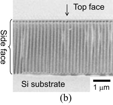 |
|
Resist Coating on Vertical Side Faces Using Conventional Spin Coating for Creating Three-Dimensional Nanostructures in Semiconductors
K. Yamazaki, and H. Yamaguchi, Applied Physics Express 3 (2010) 106501 |
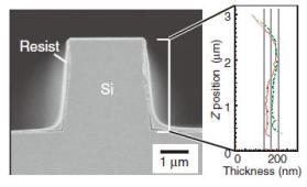 |
We have devised a new resist-coating method using spin coating for creating three-dimensional (3D) nanostructures in semiconductors. Using this method, we were able to successfully coat poly(methyl methacrylate) (PMMA) films on the vertical side faces of micrometer-order Si blocks. The use of a solvent with low viscosity was found to be effective for obtaining good uniformity in resist thickness. Moreover, Monte Carlo simulations of electron scattering revealed that fine patterning on both the opposite side faces of a Si block should be possible by simultaneous development followed by electron beam (EB) writing from opposite directions, despite electron scattering. |
|
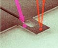
Fabrication of Nanomechanical Structures from Bulk-GaAs Using Angled Ion
Etching
V. K. Singh, K. Yamazaki, T. Tawara, H. Okamoto,and H. Yamaguchi, Applied Physics Express 2 (2009) 065001 |
| We demonstrate a novel fabrication technique for making nanomechanical structures from bulk materials with no sacrificial layer. Angled ion etching is used to suspend single- and double-clamped beams from GaAs initially. Both beams are fabricated successfully by dry anisotropic ion etching. Resonance characteristics of the fabricated beams are also investigated from 300 to 15 K. A quality factor Q of 5700 is obtained at 40 K, showing a high mechanical reliability. This technique does not rely on conventional sacrificial etching and will enable us to fabricate electro-mechanical structures from a large number of bulk materials in the micro/nano electro mechanical systems (MEMS/NEMS) field. | 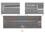 |
|
Flexible nanofabrication in three-dimensional electron-beam lithography enhanced by suppression of proximity effect
K. Yamazaki and H. Yamaguchi, Appl. Phys. Express 1, 097001 (2008) |
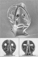 |
Nanofabrication of three-dimensional (3D) structures with a high aspect ratio has been achieved using electron-beam (EB) lithography. Although electron scattering, or the proximity effect, on the remaining parts in positive resist is generally serious for repeated EB writing from different 3D directions, we can largely avoid the effect by adding appropriate surrounding buffer regions, which are cut off by the following EB writing and development. This enables us to make a 3D nanostructure in poly(methyl methacrylate) (PMMA), which demonstrates the great structural flexibility obtainable in our EB technique. |