| |
Nanodevice's group Advanced Applied Physical Science Laboratory NTT Basic Research Laboratories |
| |
Nanodevice's group Advanced Applied Physical Science Laboratory NTT Basic Research Laboratories |
| AC-signal sensing beyond cutoff frequency using a DRAM | ||
| 37th International Microprocesses and Nanotechnology Conference (MNC 2024), Kyoto, Japan (Nov. 2024) [14D-1-3] | ||
| C. Salhani, K. Chida, T. Hayashi, and K. Nishiguchi | ||
| Electron Thermometry using Subthreshold Swing of Si Nano Transistors | ||
| 37th International Microprocesses and Nanotechnology Conference (MNC 2024), Kyoto, Japan (Nov. 2024) [14D-1-4] | ||
| H. Nayem, M. Hori, K. Nishiguchi, and Y. Ono | ||
| AC Signal-Sensing 6 Orders of Magnitude above Cutoff Frequency in DRAMs with a Non-Equilibrium Nanoscale Dot | ||
| International Conference on the Physics of Semiconductors (ICPS2024), Ottawa, Canada (Jul. 2024) [Tu-S4-6-2] | ||
| C. Salhani, K. Chida, T. Hayashi, and K. Nishiguchi | ||
| Noise Cross-Correlation Measurement of Capacitively-Coupled Silicon Nanometer-Scale Dots via Electron Counting Statistics | ||
| International Conference on the Physics of Semiconductors (ICPS2024), Ottawa, Canada (Jul. 2024) [Tu-S3-3-2] | ||
| K. Chida, A. Andrieux, and K. Nishiguchi | ||
| Energy Costs of Precise Erasure for Nanoscale Silicon Dot Memory with Non-equilibrium Initial State | ||
| International Conference on the Physics of Semiconductors (ICPS2024), Ottawa, Canada (Jul. 2024) [Mo-P-113] | ||
| T. Shimizu, K. Chida, G. Yamahata, and K. Nishiguchi | ||
| First-principal calculations for giant valley splitting in stressed silicon thin films | ||
| International Conference on the Physics of Semiconductors (ICPS2024), Ottawa, Canada (Jul. 2024) [Mo-P-064] | ||
| H. Hayashi, H. Kageshima, J. Noborisaka, and K. Nishiguchi | ||
| [Invited] Noise-to-energy conversion in silicon single-electron nanodevices | ||
| 2024 Asia-Pacific Workshop on Advanced Semiconductor Devices (AWAD 2024), Gangneung, Korea (Jul. 2024) [7-1] | ||
| K. Chida, A. Fujiwara, and K. Nishiguchi | ||
| Experimental verification of Landauer principle under a constraint of nonequilibrium initial stat | ||
| Frontiers in Non-equilibrium Physics, Kyoto, Japan (Jul. 2024) | ||
| T. Shimizu, K. Chida, G. Yamahata, and K. Nishiguchi | ||
| Electron counting statistics for observation of noise-to-energy conversion in a nanoscale dot in Gaussian noise induced nonequilibrium steady states | ||
| STATPHYS28, Tokyo, Japan (Aug. 2023) [T2a-07B-08] | ||
| K. Chida, A. Fujiwara, and K. Nishiguchi | ||
| Correlation between electric potentials in a variable-range hopping regime | ||
| STATPHYS28, Tokyo, Japan (Aug. 2023) [T4-11C-05] | ||
| T. Hayashi, Y. Tokura, and K. Nishiguchi | ||
| Application of Ambient Pressure-Driven Pumping Technology towards Ultra Low-Power Underwater Sensing | ||
| International Symposium on Underwater Technology (UT23), Tokyo, Japan (Mar. 2023) [10.3] | ||
| T. Fukuba, A. Fujiwara, K. Nishiguchi, M. Bergaud, S. Grall, S. Li, S. H. Kim, and N. Clément | ||
| Redox-labelled Electrochemical Aptasensors with Nano-supported Cancer Cells | ||
| 35th International Microprocesses and Nanotechnology Conference (MNC 2022), Tokushima, Japan(Nov. 2022) [9B-2-4] | ||
| S. Li, Y. Coffinier, C. Lagadec, F. Cleri, K. Nishiguchi, A. Fujiwara, T. Fujii, S. H. Kim, and N. Clément | ||
| Room-temperature single-electron sensor for AC signals beyond an RC time constant ~ Energy transfer via a non-leakage DRAM in non-equilibrium ~ | ||
| 35th International Microprocesses and Nanotechnology Conference (MNC 2022), Tokushima, Japan(Nov. 2022) [10B-2-1] | ||
| K. Nishiguchi, A. Fujiwara, and K. Chida | ||
| Observation of Seebeck Effect in a Silicon Electron Box by Electron Counting Statistics | ||
| International Symposium on Novel maTerials and quantum Technologies (ISNTT2021), Online (Dec. 2021) [S12-2] | ||
| K. Chida, A. Fujiwara, and K. Nishiguchi | ||
| Temperature Dependence of Low-frequency Capacitance Due to Variablerange Hopping | ||
| International Symposium on Novel maTerials and quantum Technologies (ISNTT2021), Online (Dec. 2021) [P1-07] | ||
| T. Hayashi, Y. Tokura, and K. Nishiguchi | ||
| Electron Counting Statistics for Observation of Thermoelectric Effect in a Si Electron Box | ||
| 20th International Conference on Modulated Semiconductor Structures (MSS-20), Online (Nov. 2021) [M-9-03] | ||
| K. Chida, A. Fujiwara, and K. Nishiguchi | ||
| (Invited) Single-Electron Manipulation in an Atto-Farad-Capacitor DRAM | ||
| 240th ECS Fall Meeting, Florida, US (Oct. 2021) [G02-0911] | ||
| Katsuhiko Nishiguchi, Chida Kensaku, and Akira Fujiwara | ||
| Jahn-Teller Distortion in confined DNA | ||
| 2021 International Conference on Solid State Devices and Materials (SSDM 2021), Online (Sep. 2021) [G-6-06] | ||
| I. Madrid, A. Chovin, C. Gerbelot, S. C. Grall, S. Li, T. Fujii, T. Yamaguchi, K. Nishiguchi, A. Fujiwara, S. H. Kim, A. Anne, C. Demaille, and N. Clement | ||
| Theoretical Study on Reflectometry Technique for Fast Sensing of an FET sensor | ||
| 33rd International Microprocesses and Nanotechnology Conference (MNC 2020), Online(Nov. 2020) [2020-22-19] | ||
| K. Nishiguchi and Akira Fujiwara | ||
| Nanometer-Scale Temperature Measurement Based on Single-Electron Counting Statistics in a Nanowire Si MOSFET | ||
| 33rd International Microprocesses and Nanotechnology Conference (MNC 2020), Online(Nov. 2020) [2020-22-18] | ||
| Chida Kensaku, Akira Fujiwara, and Katsuhiko Nishiguchi | ||
| Control of thermal noise originating from single-electron Brownian motion | ||
| The 6th International Symposium in Shizuoka University 2020, Shizuoka, Japan(Mar. 2020) | ||
| Katsuhiko Nishiguchi, Chida Kensaku, and Akira Fujiwara | ||
| Si-nanowire-FET sensor detecting high-frequency mechanical oscillation of a multilayer-graphene MEMS by means of reflectometry technique | ||
| 32th International Microprocesses and Nanotechnology Conference (MNC2019), Hiroshima, Japan (Oct. 2019) 30C-6-3 | ||
| K. Nishiguchi and A. Fujiwara | ||
| [ABSTRACT] A small field-effect transistor (FET) has a func-tion of a sensor with high charge sensitivity, which allows detection of single electrons. However, the FET’s smallness providing high sensitivity gives rise to difficulty of detection of fast signals because of high channel resistance of the FET. One of solutions of this problem is a reflectometry technique using the FET integrated with double LC matching circuits, which extends the detectable frequency with single-electron charge sensitivity. In this work, using an FET-based sensor com-posed of multiple Si nanowire channels, we demon-strate detection of mechanical oscillations of a mul-tilayer-graphene MEMS. Using a reflectometry technique enables de-tection of graphene’s mechanical oscillations at 240 MHz. | Link to presentation slides | |
| Information-powered operation of silicon single-electron device | ||
| International Symposium for Materials Scientists "Inspiration for Innovation by Interaction" (ISMS III), Osaka, Japan(Dec. 2018) | ||
| Chida Kensaku, Katsuhiko Nishiguchi, and Akira Fujiwara | ||
| Tunable-barrier electron pump for quantum current standards and information-to-energy converters | ||
| China-Japan International Workshop on Quantum Technologies (QTech2018), Hefei, China (Aug. 2018) | ||
| Akira Fujiwara, Gento Yamahata, and Chida Kensaku, Katsuhiko Nishiguchi | ||
| Ultimate Single Electronics with Silicon Nanowire MOSFETs | ||
| 2017 Silicon Nanoelectronics Workshop, Kyoto, Japan (Jun. 2017) | ||
| A. Fujiwara, K. Nishiguchi, G. Yamahata, and K. Chida | ||
| Electric current generation with Maxwell's demon in a Si single-electron device | ||
| 33rd International Conference on the Physics of Semiconductors (ICPS-33), Beijing, China (Aug. 2016) | ||
| Kensaku Chida, Katsuhiko Nishiguchi, and Akira Fujiwara | ||
| Gigahertz single-electron pump for quantum current standard | ||
| 33rd International Conference on the Physics of Semiconductors (ICPS-33), Beijing, China (Aug. 2016) | ||
| A. Fujiwara, G. Yamahata, K. Nishiguchi, S. P. Giblin, and M. Kataoka | ||
| Correlated phonons in a micro-nano-electromechanical system | ||
| International Symposium on Nanoscale Transport and Technology (ISNTT2015), Kanagawa, Japan (Nov. 2015) PTu03 | ||
| M. Villiers, I. Mahboob, K. Nishiguchi, D. Hatanaka, A. Fujiwara, and H.Yamaguchi | ||
| Thermal noise suppression by feedback control to single-electron motion | ||
| International Symposium on Nanoscale Transport and Technology (ISNTT2015), Kanagawa, Japan (Nov. 2015) PTu03 | ||
| K. Chida, K. Nishiguchi, G. Yamahata, H. Tanaka, and A. Fujiwara | ||
| Selective-Layer-Free Blood Ionogram Using a 0D Nanotransistor Biosensor | ||
| 28th International Microprocesses and Nanotechnology Conference (MNC2015), Toyama, Japan (Nov. 2015) 11D-2-4 | ||
| R. Sivakumarasamy, K. Nishiguchi, A. Fujiwara, and N. Clement | ||
| Fabrication of Triple-Dot Single-Electron Transistor and its Turnstile Operation | ||
| 28th International Microprocesses and Nanotechnology Conference (MNC2015), Toyama, Japan (Nov. 2015) 12P-7-31 | ||
| M. Jo, T. Uchida, A. Tsurumaki-Fukuchi, M. Arita, A. Fujiwara, Y. Ono, K. Nishiguchi, H. Inokawa, and Y. Takahashi | ||
| Electron Emission Using Multilayered-Graphene/SiO2/Si Heterodevice Driven with Low-Voltage Supply in Low Vacuum | ||
| 28th International Microprocesses and Nanotechnology Conference (MNC2015), Toyama, Japan (Nov. 2015) 13P-11-104L | ||
| D. Yoshizumi, K. Nishiguchi, Y. Sekine, K. Furukawa, A. Fujiwara, and M. Nagase | ||
| Gigahertz single-electron pump towards a representation of the new ampere | ||
| 2015 International Conference on Solid State Devices and Materials (SSDM2015), Sapporo, Japan (Sep. 2015) H-3-1 | ||
| A. Fujiwara, G. Yamahata, and K. Nishiguchi | ||
| Error detection and correction of single-electron transfer | ||
| Silicon Quantum Electronics Workshop 2015, Takamatsu, Japan (Aug. 2015) P-46 | ||
| H. Tanaka, G. Yamahata, K. Nishiguchi, and A. Fujiwara | ||
| Ultrafast single-charge transfer in silicon up to 8 GHz | ||
| Silicon Quantum Electronics Workshop 2015, Takamatsu, Japan (Aug. 2015) VII-2 | ||
| G. Yamahata, K. Nishiguchi, S. P. Giblin, M. Kataoka, and A. Fujiwara | ||
| Nanoscale Silicon MOSFET for Metrology and Valleytronics Applications | ||
| 2015 UK-Japan Silicon Nanoelectronics& Nanotechnology (UK-Japan Si NANO2), Southampton, UK (Jul. 2015) | ||
| A. Fujiwara, G. Yamahata, J. Noborisaka, and K. Nishiguchi | ||
| Gate tuning of direct optical transitions in silicon | ||
| 2015 Asia-Pacific Workshop on Fundamentals and Applications of Advanced Semiconductor Devices (AWAD2015), Jeju Island, Korea (Jul. 2015) Tu-A3-4 | ||
| J. Noborisaka, K. Nishiguchi, and A. Fujiwara | ||
| Gigahertz single-electron transfer via a single-trap level in silicon | ||
| 21st International Conference on Electronic Properties of Two-Dimensional Systems (EP2DS-21), Sendai, Japan (Jul. 2015) Tu-A3-4 | ||
| G. Yamahata, K. Nishiguchi, M. Kataoka, and A. Fujiwara | ||
| What happens in a small transistor with single-electron resolution? | ||
| The 5th International Symposium on Organic and Inorganic Electronic Materials and Related Nanotechnologies (EM-NANO 2015), Niigata, Japan (Jun. 2014) | ||
| K. Nishiguchi | ||
| [ABSTRACT] Downscaling of silicon transistors using state-of-the-art technology has already reached 20~16-nm generation and enabled massive productions of high-performance electrical circuits for various applications. Such downscaling also provides transistors with new functionalities: single-electron transfer and detection at room temperature. This couple of functions allows new applications utilizing single electrons. | Link to presentation slides | |
| Violation of equipartition of energy in thermal noise of a small DRAM | ||
| 27th International Microprocesses and Nanotechnology Conference (MNC 2014), Fukuoka, Japan (Nov. 2014) | ||
| K. Nishiguchi and A. Fujiwara | ||
| [ABSTRACT] we introduce a transition between the valid and invalid law of equipartition of energy in thermal noise in a small DRAM. We analyzed Brownian motion, i.e., thermal noise, of single electrons entering and exiting a small capacitor whose charging energy Ec is comparable to thermal energy kT. When Ec>kT, the electron motion is suppressed due to the violation of the law of equipartition of energy. | Link to presentation slides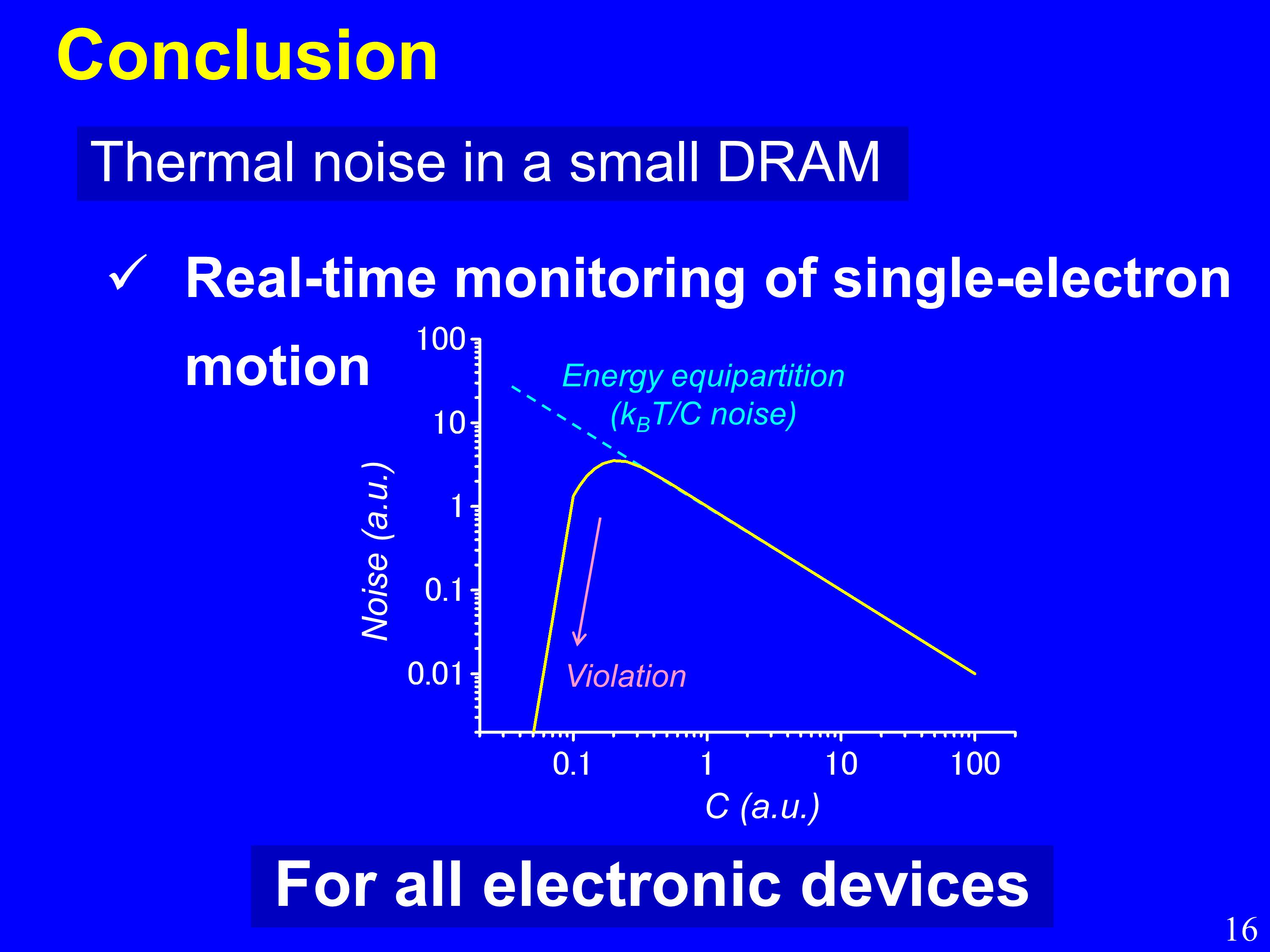 | |
| Tunnel diode composed of MoS2/SiO2/Si heterojunction | ||
| 27th International Microprocesses and Nanotechnology Conference (MNC 2014), Fukuoka, Japan (Nov. 2014) | ||
| K. Nishiguchi,A. Castellanos-Gomez, H. Yamaguchi, A. Fujiwara, H. S. J. van der Zant, and G. A. Steele | ||
| [ABSTRACT] we introduce a tunnel diode based on a combination of MoS2 with a Si MOSFET. An n-type-MoS2/SiO2/p-type-Si heterostructure provides current characteristics with negative differential resistance (NDR) reflecting the number of the MoS2 layers. | Link to presentation slides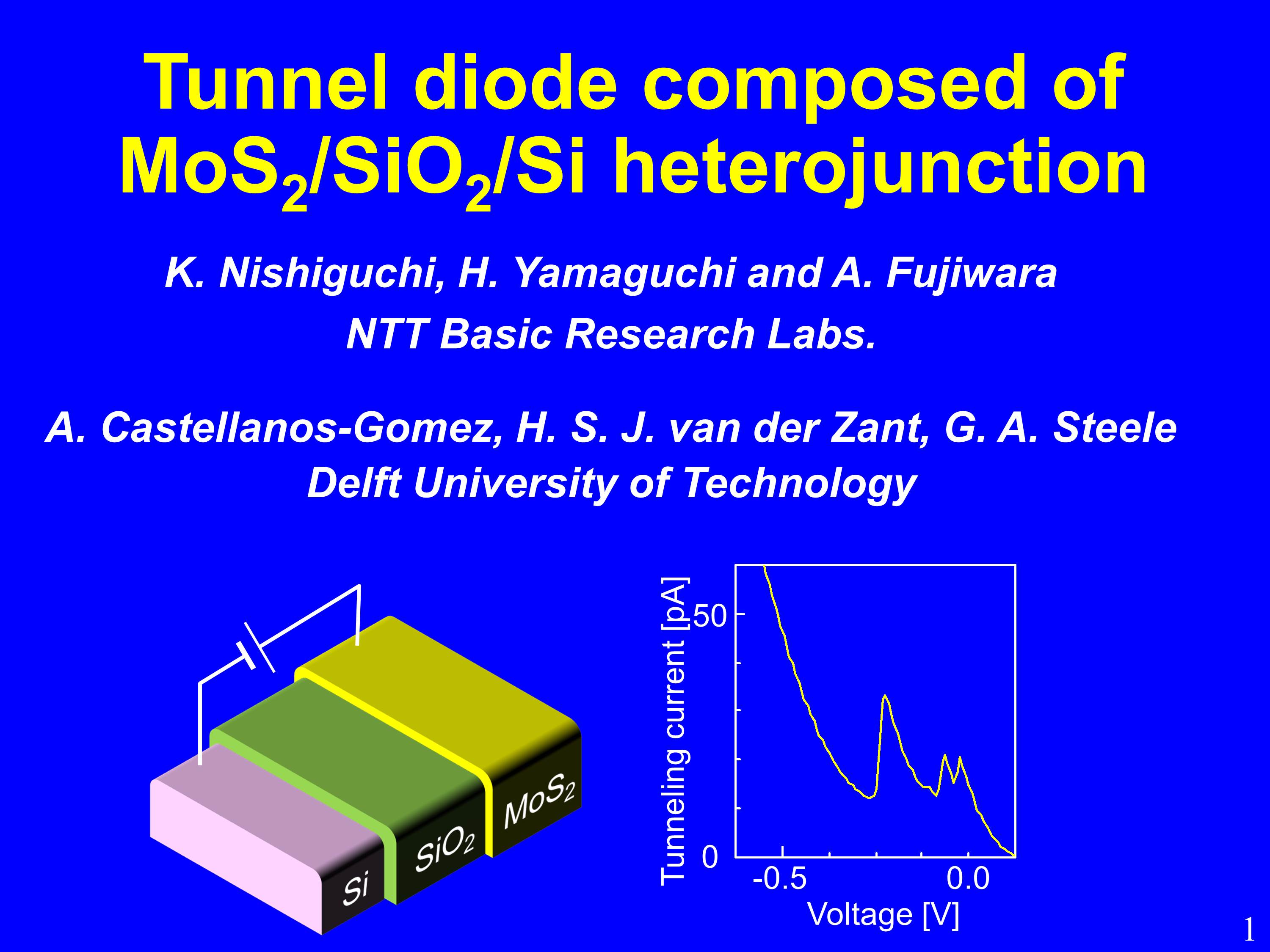 | |
| Phonon-lasing (and mode cooling) in an electromechanical resonator | ||
| 27th International Microprocesses and Nanotechnology Conference (MNC 2014), Fukuoka, Japan (Nov. 2014) (Aug. 2014) | ||
| Imran Mahboob, K. Nishiguchi, A. Fujiwara, and H. Yamaguchi | ||
| Zero Dimensional Ion-Sensitive Field-Effect Transistors | ||
| 27th International Microprocesses and Nanotechnology Conference (MNC 2014), Fukuoka, Japan (Nov. 2014) (Aug. 2014) | ||
| R. Sivakumarasamy, K. Nishiguchi, A. Fujiwara, D. Vuillaume, and N. Clement | ||
| Thermal-Noise Suppression in Nanometer-Scale Si Field-Effect Transistors by Feedback Control with Single-Electron Resolution | ||
| 2014 Solid State Devices and Materials (SSDM2014), Tsukuba, Japan (Sep. 2014) | ||
| K. Chida, K. Nishiguchi, G. Yamahata, and A. Fujiwara | ||
| Enhanced inter-band dipole transition due to large valley splitting at the Si/SiO2 interface | ||
| Silicon Quantum Electronics Workshop, New Mexico, USA (Aug. 2014) | ||
| J. Noborisaka, K. Nishiguchi, and A. Fujiwara | ||
| Silicon nanowire MOSFETs for diverse applications | ||
| The 6th IEEE International Nanoelectronics Conference (IEEE INEC2014), Sapporo, Japan (Jul. 2014) | ||
| A. Fujiwara, K Nishiguchi, and G. Yamahata | ||
| Water electrolysis and energy harvesting with 0D Ion-Sensitive Field-Effect Transistors | ||
| The 1st International Symposium on Energy Challenges & Mechanics (ECM2014), Scotland, UK (Jul. 2014) | ||
| N. Clement, K Nishiguchi, J-F Dufreche, D. Guerin, A. Fujiwara, and D. Vuillaume | ||
| Mechanism crossover of single-electron transfer in Si tunable-barrier turnstiles | ||
| The International Symposium on Nanoscale Transport and Technology (ISNTT2013), Kanagawa, Japan (Nov. 2013) | ||
| G. Yamahata, K. Nishiguchi, and A. Fujiwara | ||
| A nanoelectromechanical resonator embedded in a microelectromechanical resonator | ||
| The International Symposium on Nanoscale Transport and Technology (ISNTT2013), Kanagawa, Japan (Nov. 2013) | ||
| N. Perrissin, I. Mahboob, K. Nishiguchi, D. Hatanaka, Y. Okazaki, A. Fujiwara and H. Yamaguchi | ||
| Multimode parametric resonance dynamics in an electromechanical resonator | ||
| The International Symposium on Nanoscale Transport and Technology (ISNTT2013), Kanagawa, Japan (Nov. 2013) | ||
| I. Mahboob, M. Mounaix, K. Nishiguchi, A. Fujiwara and H. Yamaguchi | ||
| High-charge-sensitivity radio-frequency field-effect transistor with large and tunable readout frequency | ||
| 26th International Microprocesses and Nanotechnology Conference (MNC 2013), Sapporo, Japan (Nov. 2013) | ||
| K. Nishiguchi,H. Yamaguchi, A. Fujiwara, H. S. J. van der Zant, and G. A. Steele | ||
| [ABSTRACT] We introduce the RF-FET composed of double LC matching circuits. The double matching circuits provide an additional resonance condition tuned by a variable capacitor, which allows the extension of the readout frequency to 200 MHz. | Link to presentation slides | |
| Ultimate Integration of a PDMS-Based Lab-on-a-Chip with Nanotransistor Bio-sensors | ||
| 26th International Microprocesses and Nanotechnology Conference (MNC 2013), Sapporo, Japan (Nov. 2013) | ||
| R. Sivakumarasamy, K. Nishiguchi, A. Fujiwara, D. Vuillaume, and N. Clement | ||
| Dual-gate Silicon Single-Electron Transistor Threshold Voltage mapping at Nanoscale with a Scanning Microwave Microscope | ||
| 26th International Microprocesses and Nanotechnology Conference (MNC 2013), Sapporo, Japan (Nov. 2013) | ||
| N. Clement, F. Wang, K. Nishiguchi, A. Fujiwara, G. Patriarche, D. Troadec, B. Legrand, G. Dambrine and D. Theron | ||
| Dielectric Polarization 1/f Noise: a signature of defect-free oxides at nanotransistors interface | ||
| APS March Meeting, Maryland, USA (Mar. 2013) | ||
| N. Clement, K. Nishiguchi, D. Vuillaume, and A. Fujiwara | ||
| Interferometric Scanning Microwave Microscope for Nanotechnology Application | ||
| APS March Meeting, Maryland, USA (Mar. 2013) | ||
| N. Clement, T. Dargent, H. Tanbakuchi, K. Nishiguchi, R. Sivakumarasamy, F. Wang, A. Fujiwara, D. Ducatteau, G. Dambrine, D. Vuillaume, B. Legrand, and D. Theron | ||
| Transducing Energy Loss in Water Electrolysis with a 0D Ion-Sensitive Field-Effect Transistor | ||
| APS March Meeting, Maryland, USA (Mar. 2013) | ||
| N. Clement, K. Nishiguchi, J-F. Dufreche, D. Guerin, G. Patriarche, D. Troadec, A. Fujiwara, and D. Vuillaume | ||
| Single-electron counting statistics of shot and thermal noise in nanowire Si MOSFET [Invited] | ||
| Nanosciences Fondation-Quantum Nanoelectronics Seminar-, Grenoble, France (Feb. 2013) | ||
| K. Nishiguchi | ||
| Crossover of transfer mechanism in Si single-electron turnstiles | ||
| 2013 International Workshop On Silicon Quantum Electronics, Grenoble, France (Feb. 2013) | ||
| G. Yamahata, K. Nishiguchi, and A. Fujiwara | ||
| Silicon Single-Electron Transfer Devices: Ultimate Control of Electric Charge | ||
| 2012 Silicon Nanoelectronics Workshop, Honolulu, USA (Jun. 2012) | ||
| A. Fujiwara, G. Yamahata, K. Nishiguchi, G. P. Lansbergen, and Y. Ono | ||
| High-frequency properties of Si single-electron transistor | ||
| 2012 Silicon Nanoelectronics Workshop, Honolulu, USA (Jun. 2012) | ||
| H. Takenaka, M. Shinohara, T. Uchida, M. Arita, A. Fujiwara, Y. Ono, K. Nishiguchi, H. Inokawa, and Y. Takahashi | ||
| One-by-One H2 Bubble Counting during Water Electrolysis with a Chemical Electrometer | ||
| 2012 MRS Spring Meeting, San Francisco, USA (Apr. 2012) | ||
| N. Clement, K. Nishiguchi, J-F Dufreche, D. Guerin, A. Fujiwara, D. Vuillaume | ||
| Stochastic resonance using a steep-subthreshold-swing transistor | ||
| 24th International Microprocesses and Nanotechnology Conference (MNC 2011), Kyoto, Japan (Oct. 2011) | ||
| K. Nishiguchi and A. Fujiwara | ||
| [ABSTRACT] We demonstrated stochastic resonance (SR) by using a FET whose characteristics have a strong nonlinearity and hysteresis, which allows a higher SR response. Additionally, encoding and decoding for an image-pattern hiding was also demonstrated. | Link to presentation slides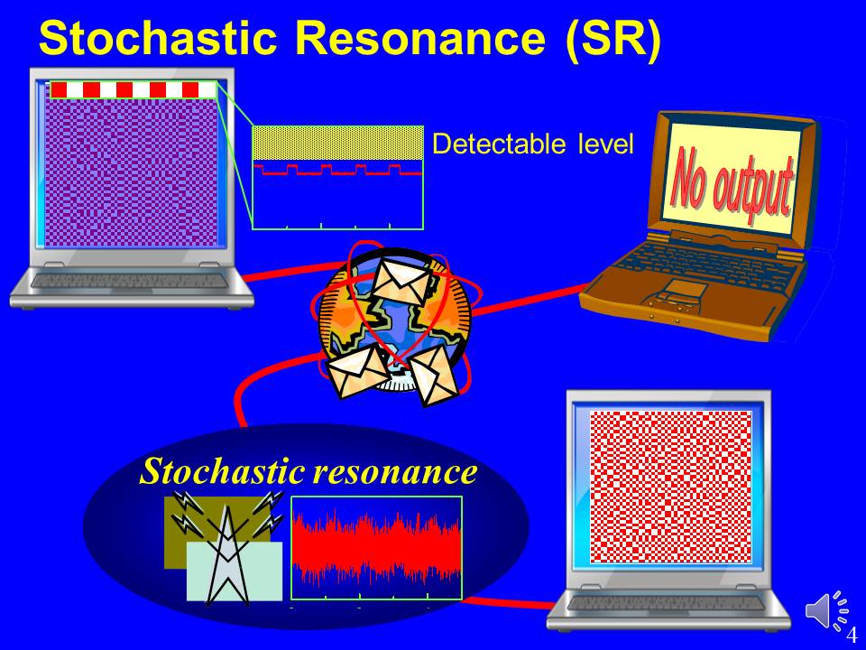 | |
| Mechanical idler generation | ||
| 2011 International Conference on Solid State Devices and Materials, Nagoya, Japan (Sep. 2011) | ||
| I. Mahboob, Q. Wilmart, K. Nishiguchi, A. Fujiwara and H. Yamaguchi | ||
| Accuracy of Single-electron Shuttle Transfer in Si Nanowire MOSFETs | ||
| 19th international conference on Electronic Properties of Two-Dimensional Systems (EP2DS19), Florida, USA (Jul. 2011) | ||
| G. Yamahata, K. Nishiguchi, and A. Fujiwara | ||
| Observation of New Current Peaks of Si Single-Electron Transistor with a Single-Hole Trap | ||
| Silicon Nanoelectronics Workshop 2011, Honolulu, USA (Jun. 2011) | ||
| M. Sinohara, Y. Kato, M. Arita, A. Fujiwara, Y. Ono, K. Nishiguchi, H. Inokawa, and Y. Takahashi, | ||
| Shuttling Transfer of Single Electrons in Si Nanowire MOSFETs | ||
| International Symposium on Nanoscale Transport and Technology (ISNTT2011), Atsugi, Japan (Jan. 2011) | ||
| G. Yamahata, K. Nishiguchi, and A. Fujiwara | ||
| Single-electron stochastic resonance using Si nano-wire transistors | ||
| International Symposium on Nanoscale Transport and Technology (ISNTT2011), Atsugi, Japan (Jan. 2011) | ||
| K. Nishiguchi and A. Fujiwara | ||
| [ABSTRACT] We demonstrated SE-based stochastic resonance (SR) using nanoscale MOSFETs. The correlation between input and output signals are enhanced by thermal noise. Moreover, it is confirmed that a parallel SR system allows further enhancement of the correlation. This is very useful for practical applications because optimization of added noise becomes easy and robustness to fluctuation of the electrical charac-teristics of nanoscale MOSFETs is guaranteed. | Link to presentation slides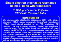 | |
| Single-electron applications using nano-wire MOSFETs [invited] | ||
| 2010 Workshop on Innovative Devices and Systems (WINDS), Hawaii, USA (Dec. 2010) | ||
| K. Nishiguchi and A. Fujiwara | ||
| [ABSTRACT] A MOSFET-based circuit utilizing single electrons is demonstrated at room temperature. A nano-wire MOSFET can transfer a single electron one after another to a storage node thanks to extremely small current leakage of the MOSFET. The electrons transferred to the node are detected by another wire MOSFET which is located near the node. The combination of these nano-wire MOSFETs allows a real-time monitoring of single-electron transfer, which helps microscopic understanding of individual electron movement in the MOSFET. While the MOSFET can control an average movement of single electrons, each movement of an individual electron is completely random. Such controllability and randomness of electron movement is used for high-quality random-number generation (RNG) suitable for a data processing which stochastically extracts the most preferable pattern among various ones. The MOSFET-based RNG allows fast operation as well as high controllability, which leads to flexible extraction of the preferable pattern. This stochastic data processing promises high efficiency, fast operation, and low power consumption as a human brain. | Link to presentation slides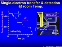 | |
| Fast sensing using single-electron stochastic resonance in Si nano-wire transistors | ||
| 23rd International Microprocesses and Nanotechnology Conference (MNC 2010), Kokura, Japan (Nov. 2010) | ||
| K. Nishiguchi and A. Fujiwara | ||
| [ABSTRACT] We demonstrated SE-based stochastic resonance (SR) using nanoscale MOS-FETs. The physical nature of shot noise represented by single-electron random movement allows fast SR dem-onstration, which leads to time-division SR operation with one unit instead of multiple network units. This is very useful for high integrability of sensors and for single-shot sensing of quickly moving targets. | Link to presentation slides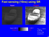 | |
| Body-biased steep-subthreshold-swing MOS (BS-MOS) with small hysteresis, off current, and drain voltage | ||
| 2010 International Conference on Solid State Devices and Materials (SSDM 2010), Tokyo, Japan (Sep. 2010) | ||
| K. Nishiguchi and A. Fujiwara | ||
| [ABSTRACT] We demonstrate a 30-nm-gate-length nanowire MOSFET with steep subthreshold swing (SS). A parasitic bipolar transistor (PBT) formed in a fully depleted SOI MOSFET applies body bias (BB) to the MOSFET’s channel and thus reduces the SS below 60 mV/dec at room temperature. Additionally, triple-gate operation allows current characteristics with small hysteresis, a high on/off ratio, and low drain voltage. These features promise SOI MOSFETs for low power consumption. | Link to presentation slides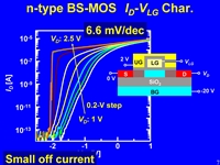 | |
| Strong Stark effect of electroluminescence in thin SOI MOSFETs | ||
| 2010 International Conference on Solid State Devices and Materials (SSDM 2010), Tokyo, Japan (Sep. 2010) | ||
| J. Noborisaka, K. Nishiguchi, Y. Ono, H. Kageshima, and A. Fujiwara | ||
| Analysis of Tunneling Potential of Si SETs Fabricated by Pattern-Dependent Oxidation | ||
| 2010 Silicon Nanoelectronics Workshop, Tokyo, Japan (Sep. 2010) | ||
| Y. Kato, M. Jo, M. Arita, A. Fujiwara, Y. Ono, K. Nishiguchi, H. Inokawa, Y. Takahashi and J.-B. Choi | ||
| Single-Electron Stochastic Resonance using Si Nano-Wire Transistors | ||
| 22th International Microprocesses and Nanotechnology Conference (MNC 2009), Sapporo, Japan (Nov. 2009) | ||
| K. Nishiguchi, S. Miyamoto and A. Fujiwara | ||
| [ABSTRACT] We demonstrated SE-based SR using nanoscale MOS-FETs. The correlation between input and output signals are enhanced by adding noise. Moreover, it is confirmed that a parallel SR system allows further enhancement of the correlation. This is very useful for practical applications because optimization of added noise becomes easy and robustness to fluctuation of the electrical characteristics of nanoscale MOSFETs is guaranteed. SE-based SR would also be useful for the analysis of individual-electron behavior in an electrically defined quantum dot. | Link to presentation slides | |
| Single-electron Counting Statistics of Shot Noise in Nanowire Si MOSFETs | ||
| 2009 International Conference on Solid State Devices and Materials (SSDM 2009), Sendai, Japan (Oct. 2009) | ||
| K. Nishiguchi, Y. Ono, and A. Fujiwara | ||
| [ABSTRACT] Shot noise in the transport of single electrons in a Si metal-oxide-semiconductor field-effect transistor is monitored by real-time measurement with a high-charge-sensitivity electrometer. In the current range between zepto and attoamperes, the current characteristics are found to be divided into two regimes: a temperature-independent regime in the lower current range and a temperature-dependent one in the higher current range. A time-domain analysis reveals that, for both regimes, the single-electron transport obeys a pure Poisson process with the Fano factor’s being nearly unity, while the shot noise is suppressed with reduced Fano factors around the boundary. | Link to presentation slides | |
| Single-electron-based stochastic circuit for pattern recognition using nano-FETs | ||
| International Symposium on Nanoscale Transport and Technology (ISNTT2009), Atsugi, Japan (Jan. 2009) | ||
| K. Nishiguchi and A. Fujiwara | ||
| [ABSTRACT] A MOSFET-based circuit utilizing single electrons is demonstrated at room temperature. Individual electrons randomly passing through the nanoscale MOSFET are monitored by an electrometer in real time. Such a random behavior of single electrons (SEs) is used for high-quality random-number generation (RNG) suitable for a data processing which stochastically extracts the most preferable pattern among various ones. The MOSFET-based RNG allows fast operation as well as high controllability, which leads to flexible extraction of the preferable pattern. | Link to presentation slides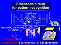 | |
| Fabrication of triple-dot single-electron transistor and its single-electron-transfer operation | ||
| 2009 International Symposium on Advanced Nanodevices and Nanotechnology (ISANN 2009), Sendai, Japan (Oct. 2009) | ||
| M. Jo, Y. Kato, M. Arita, A. Fujiwara, Y. Ono, K. Nishiguchi, H. Inokawa, Y. Takahashi, and J-B Choi | ||
| Identification of Single Boron Acceptors in Nanowire MOSFETs | ||
| 2009 International Conference on Solid State Devices and Materials (SSDM 2009), Sendai, Japan (Oct. 2009) | ||
| Y. Ono, M. A. H. Khalafalla, S. Horiguchi, K. Nishiguchi, and A. Fujiwara | ||
| Tunnel Spectroscopy of Electron Subbands in Thin SOI MOSFETs | ||
| 2009 International Conference on Solid State Devices and Materials (SSDM 2009), Sendai, Japan (Oct. 2009) | ||
| J. Noborisaka, K. Nishiguchi, H. Kageshima, Y. Ono, and A. Fujiwara | ||
| Random Telegraph Signal and Low Frequency Noise in Silicon Charge-Sensitive Electrometers | ||
| 2009 International Conference on Solid State Devices and Materials (SSDM 2009), Sendai, Japan (Oct. 2009) | ||
| N. Clement, K. Nishiguchi, A. Fujiwara, and D. Vuillaume | ||
| Single-electron activation over an oscillating barrier in silicon nanowire MOSFETs | ||
| EP2DS-2, Kobe, Japan (Jul. 2009) | ||
| S. Miyamoto, K. Nishiguchi, Y. Ono, K. M. Itoh, and A. Fujiwara | ||
| Electron-hole transport in a 40 nm thick silicon slab | ||
| EP2DS-2, Kobe, Japan (Jul. 2009) | ||
| K. Takashina, K. Nishiguchi, Y. Ono, A. Fujiwara, T. Fujisawa, Y. Hirayama, and K. Muraki | ||
| Position Analysis of Single Acceptors in Si Nanoscale Field-Effect Transistors | ||
| 2009 Silicon Nanoelectronics Workshop, Kyoto, Japan (Jun. 2009) | ||
| Khalafalla, Y. Ono, K. Nishiguchi, and A. Fujiwara | ||
| Fabrication of Coupled-Dot Single-Electron Transistor in Silicon Nanowire | ||
| 2009 Silicon Nanoelectronics Workshop, Kyoto, Japan (Jun. 2009) | ||
| M. Jo, T. Kaizawa, M. Arita, A. Fujiwara, Y. Ono, K. Nishiguchi, H. Inokawa, Y. Takahashi, and J.-B. Choi | ||
| Si nano-wire ion-sensitive field-effect transistors with a shared floating gate | ||
| 21th International Microprocesses and Nanotechnology Conference (MNC 2008), Fukuoka, Japan (Oct. 2008) | ||
| K. Nishiguchi, N. Clement, Y. Yamaguchi, and A. Fujiwara | ||
| [ABSTRACT] Ion-sensitive field-effect transistors (ISFETs) arrayed in parallel were fabricated on a silicon-on-insulator substrate. Since the nanoscale wire channels of the ISFETs are bridged with a floating gate, on which molecules are preferably immobilized, signals originating from charged materials only on the floating gate can appear and can therefore be distinguished from background noise, which leads to noise-robust sensing. Additionally, the nanoscale channels provide the ISFETs with single-electron-resolution charge sensitivity as well as a reduction of background noise induced in the wider channels used as electrical leads. These features promise the detection of a small number of molecules. | Link to presentation slides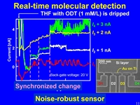 | |
| Single-electron-resolution electrometer based on field-effect transistor | ||
| 2008 Asia-Pacific Workshop on Fundamental and Application of Advanced Semiconductor Devices (AWAD), Sapporo, Japan (Jul. 2008) | ||
| K. Nishiguchi, C. Koechlin, Y. Ono, A. Fujiwara, H. Inokawa, and H. Yamaguchi | ||
| [ABSTRACT] An electrometer based on a field-effect transistor was fabricated on a silicon-on-insulator substrate. The electrometer has an extremely small channel and a capacitively coupled node, where single electrons are stored. Dependences of the charge sensitivity of the electrometer on its geometry and on its operation condition were evaluated which enabled the electrometer to have extremely high charge sensitivity, 0.002 e/Hz^0.5 @ 7Hz, at room temperature. | Link to presentation slides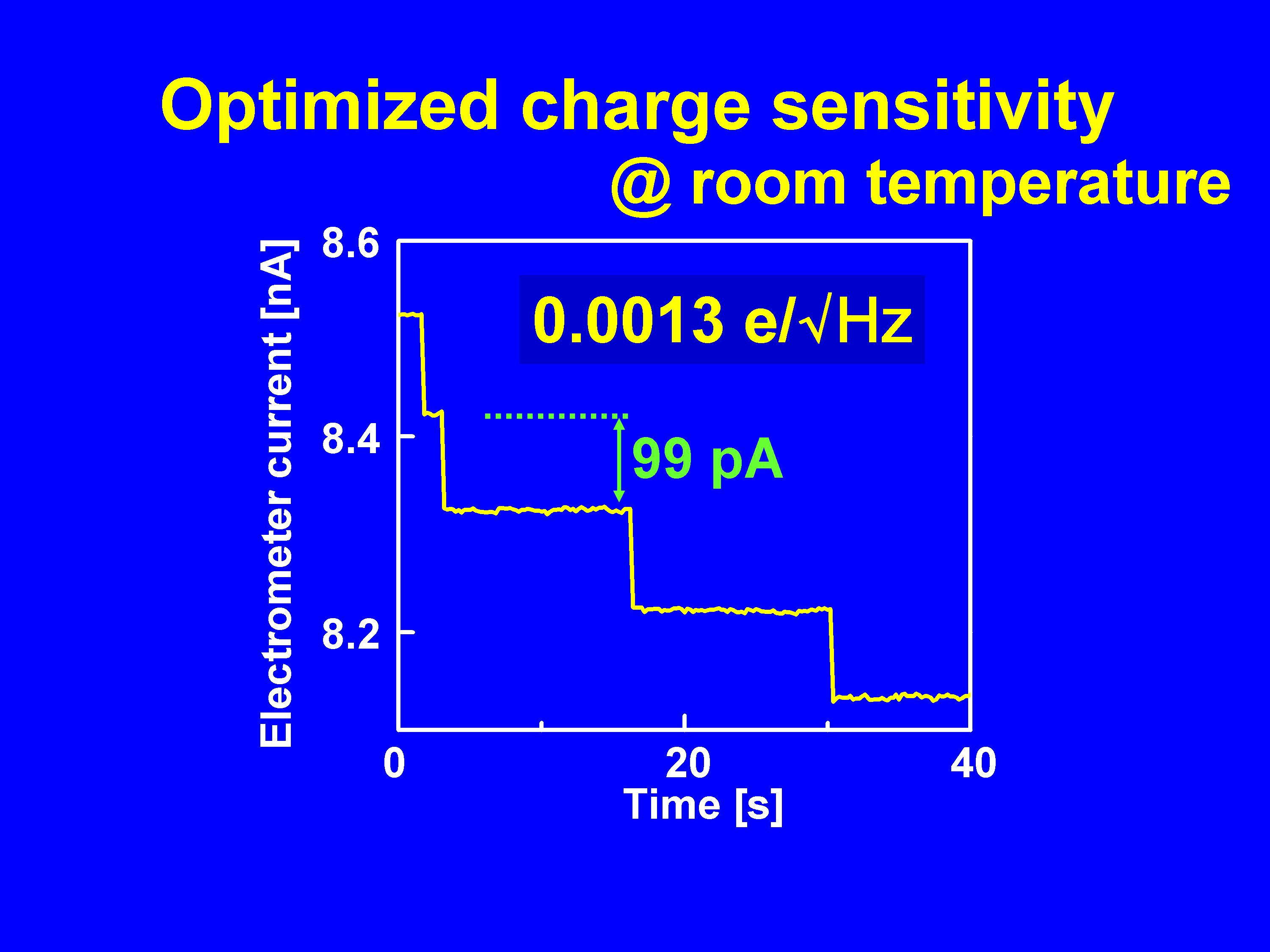 | |
| Dynamics of Single-Electron Capture in Si Nanowire MOSFETs | ||
| Silicon Nanoelectronics Workshop 2008, Honolulu, USA (Jun. 2008). | ||
| A. Fujiwara, S. Miyamoto, K. Nishiguchi, Y. Ono, and N. M. Zimmerman. | ||
| Single-electron circuit for stochastic data processing using nano-MOSFETs | ||
| International Electron Devices Meeting (IEDM), Washington, USA (Dec. 2007) | ||
| K. Nishiguchi and A. Fujiwara | ||
| [ABSTRACT] A MOSFET-based circuit utilizing single electrons is demonstrated at room temperature. Individual electrons randomly passing through the nanoscale silicon-on-insulator (SOI) MOSFET are monitored by an electrometer in real time. Such a random behavior of single electrons is used for random-number generation suitable for a data processing which stochastically extracts the optimum solution among various ones. MOSFET-based electron transport provides high controllability of the randomness, which prevents extracted solutions from staying at undesirable local minimum, as well as fast generation of random numbers. The present result promises new single-electron applications using nanoscale MOSFETs. | Link to presentation slides | |
| Low-energy electron emission using a Si/SiO2/Si cathode for nano-decomposition | ||
| 20th International Microprocesses and Nanotechnology Conference (MNC 2007), Kyoto, Japan (Nov. 2007) | ||
| K. Nishiguchi, M. Nagase, T. Yamaguchi, A. Fujiwara, and H. Yamaguchi | ||
| [ABSTRACT] We fabricated an electron-emission cathode with a Si/SiO2/Si structure using metal-oxide-semiconductor field-effect transistor (MOSFET) fabrication technology. Electrons travel from an electron-source Si layer to a thin polycrystalline Si (poly-Si) through a thin SiO2 and some of them with high energy, i.e., hot electrons, are emitted from the poly-Si surface. By utilizing an electron-inversion layer as the electron source, high efficiency and stability of electron emission were achieved. Material decomposition at a depth of a few nanometers was also demonstrated using a low-energy-electron irradiation from the cathode operated in a low vacuum condition. | Link to presentation slides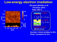 | |
| Room-temperature-operating single-electron devices using silicon nanowire MOSFET [invited] | ||
| 2007 Asia-Pacific Workshop on Fundamentals and Applications of Advanced Semiconductor Devices (AWAD) | ||
| K. Nishiguchi, Y. Ono, A. Fujiwara, H. Inokawa, and Y. Takahashi | ||
| [ABSTRACT] In this paper, we report the development of devices for single-electron transfer and detection at room temperature, using silicon (Si) metal-oxide-semiconductor field-effect transistors (MOSFETs). Single electrons are transferred to a storage node (SN) by modulating the potential barrier in the channel of the MOSFETs. Another MOSFET, located close to the SN, detects electrons transferred into the SN with single-electron resolution. These transfer and detection functions were applied to a digital-to-analog converter, gain-cell memory, and infrared sensor. | Link to presentation slides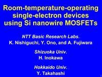 | |
| Charge Transport in Boron-Doped Nano MOSFETs: Towards Single-Dopant Electronics | ||
| Fifth International Symposium on Control of Semiconductor Interfaces (ISCSI ・V), Tokyo, Japan (Nov. 2007). | ||
| Y. Ono, M. Khalafalla, K. Nishiguchi, K. Takashina, and A. Fujiwara. | ||
| A Simple Test Structure for Extracting Capacitances in Nanometer-Scale MOSFETs | ||
| The 6-th annual International Conference on Global Research and Education(inter academia), Hamamatsu, Japan (Sep. 2007, Hamamatsu). | ||
| H. Inokawa, A. Fujiwara, K. Nishiguchi, Y. Ono, and H. Satoh. | ||
| Identification of Single and Coupled Acceptors in Silicon Nano Field-Effect Transistors | ||
| 2007 International Conference on Solid State Devices and Materials (SSDM), Tsukuba, Japan (Sep,2007). | ||
| M. Khalafalla, Y. Ono, K. Nishiguchi, and A. Fujiwara. | ||
| Capacitive Parameter Extraction for Nanometer-Size Field-Effect Transistors | ||
| 2007 International Conference on Solid State Devices and Materials (SSDM), Tsukuba, Japan (Sep,2007) | ||
| H. Inokawa, A. Fujiwara, K. Nishiguchi, and Y. Ono. | ||
| Nanoampere charge pumping by single-electron ratchet using Si nanowire MOSFETs | ||
| 2007 International Conference on Solid State Devices and Materials (SSDM), Tsukuba, Japan (Sep,2007). | ||
| A. Fujiwara, K. Nishiguchi, and Y. Ono. | ||
| Single-electron ratchet using silicon nanowie MOSFET | ||
| International Conference on Electronic Properties of Two-dimensional Systems and Modulated Semiconductor Structures (EP2DS 17 + 13 MSS), Genova, Italy (Jul. 2007). | ||
| A. Fujiwara, K. Nishiguchi, and Y. Ono. | ||
| Dopant-mediated charge transport in boron-doped nano MOSFETs | ||
| 2007 Silicon Nanoelectronics Workshop (SNW), Kyoto, Japan (Jun. 2007). | ||
| Y. Ono, M. Khalafalla, K. Nishiguchi, K. Takashina, H. Yamaguchi, A. Fujiwara, S. Horiguchi, H. Inokawa, and Y. Takahashi. | ||
| Recent progress in integration of silicon single-electron devices [invited] | ||
| The 4th International Workshop on Ubiquitous Knowledge Network Environment , Sapporo, Japan (Mar. 2007). | ||
| H. Inokawa , K. Nishiguchi, Y. Ono, A. Fujiwara, and Y. Takahashi. | ||
| Hopping conduction in buried-channel SOI MOSFETs with shallow impurities | ||
| International Conference on Nanoelectronics, Nanostructures, and Carrier Interaction (NNCI) 2007, Kanagawa, Japan (Feb. 2007). | ||
| Y. Ono, J.-F. Morizur, K. Nishiguchi, K. Takashina, H. Yamaguchi, A. Fujiwara, K. Hiratsuka, S. Horiguchi, H. Inokawa, and Y. Takahashi. | ||
| Infrared detection with silicon nano transistors | ||
| Solid State Devices and Materials (SSDM) 2006 | ||
| K. Nishiguchi, Y. Ono, A. Fujiwara, H. Yamaguchi, H. Inokawa, and Y. Takahashi | ||
| [ABSTRACT] In this paper, we report IR sensing using nano-scale Si MOSFETs. An IR signal excites conduction-band majority electrons and some of them are injected into a memory node (MN) electrically formed by a MOSFET. Small signal originating from electrons stored in the MN are detected by an electrometer with single-electron resolution. Additionally, the MOSFET controls the number and energy of electron for injection to the MN. This leads to the electrical control of the sensitivity, suggesting the possibility of highly functional IR sensors. | Link to presentation slides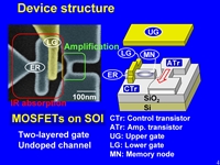 | |
| Transfer and detection of single-electron using metal-oxide-semiconductor field-effect transistors | ||
| 2006 Asia-Pacific Workshop on Fundamental and Application of Advanced Semiconductor Devices (AWAD) | ||
| W. C .Zhang, K. Nishiguchi, Y. Ono, A. Fujiwara, H. Yamaguchi, H. Inokawa, Y. Takahashi, and N. J. Wu | ||
| [ABSTRACT] A single-electron turnstile and electrometer circuit was fabricated on a silicon-on-insulator substrate. The turnstile, which is operated by opening and closing two metal-oxide-semiconductor field-effect-transistors (MOSFETs) alternately, allows current quantization at 20K due to single-electron transfer. Another MOSFET is placed at the drain side of the turnstile to form an electron storage island. Therefore, one-by-one electron entrance into the storage island from the turnstile can be detected as an abrupt change in the current of the electrometer, which is placed near the storage island and electrically coupled to it. The correspondence between the quantized current and the single-electron counting was confirmed. | Link to presentation slides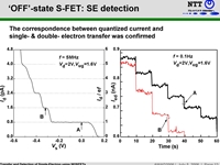 | |
| Room-Temperature Operation of Data Processing Circuit Based on Single-Electron Transfer and Detection with Metal-Oxide-Semiconductor Field-Effect-Transistor Technology | ||
| Silicon Nanoelectronics Workshop 2006 | ||
| K. Nishiguchi, A. Fujiwara, Y. Ono, H. Inokawa, and Y. Takahashi | ||
| [ABSTRACT] A single-electron-based circuit was fabricated using SOI MOSFET technology. The fabricated circuit includes functions for both single-electron transfer and detection. The turnstile, which transfers electrons one by one by opening and closing two MOSFETs alternately, achieves room-temperature operation owing to electric-field-assisted shrinkage of the single-electron box. We demonstrated a time-division weighted sum circuit for a digital-to-analog (DA) converter. | Link to presentation slides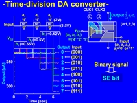 | |
| Long-Retention Gain-Cell DRAM Using Undoped SOI MOSFET | ||
| Silicon Nanoelectronics Workshop 2006 | ||
| K. Nishiguchi, A. Fujiwara, Y. Ono, H. Inokawa, and Y. Takahashi | ||
| [ABSTRACT] A gain-cell (GC-) DRAM was fabricated using 20-nm-gate-length SOI MOSFET. Since a memory node is electrically formed in an undoped narrow channel by a two-layered gate, pn-junction leakage is suppressed, which leads to long data retention (~10^4 s @ 85°C). The operation for data writing, whose procedure is the same as that for a conventional DRAM, allows writing time of 10 ns. High compatibility of the fabrication process with those of SOI MOSFETs should enable us to embed the GC-DRAM into logic LSIs . | Link to presentation slides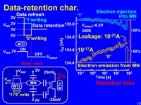 | |
| Metal-Oxide-Semiconductor-Based Single-Electronics | ||
| The 5-th annual International Conference on Global Research and Education (inter-Academia), Iasi, Romania (Sep. 2006). | ||
| H. Inokawa, K. Nishiguchi, A. Fujiwara, Y. Ono, Y. Takahashi, and H. Yamaguchi. | ||
| Impurity conduction and its control in phosphorus-doped SOI MOSFET [invited] | ||
| 2006 Silicon Nanoelectronics Workshop (SNW), Honolulu, USA (Jun. 2006). | ||
| Y. Ono, K. Nishiguchi, K. Takashina, H. Inokawa, S. Horiguchi, andY. Takahashi. | ||
| Back-gate effect on Coulomb blockade in SOI trench wires | ||
| Silicon Nanoelectronics Workshop 2005 | ||
| K. Nishiguchi, O. Crauste, H. Namatsu, S. Horiguchi, Y. Ono, A. Fujiwara, H. Inokawa, and Y. Takahashi | ||
| [ABSTRACT] A back-gate (BG) effect on a Coulomb blockade (CB) in a SOI nanowire at the trench bottom is investigated. Negative BG voltage increases charging energy of the Coulomb island in the nanowire. This indicates the possibility that the BG voltage shifts electron wave functions in the source/drain area away from the nanowire and decreases the capacitances of small junctions located at both ends of it. | Link to presentation slides | |
| Single-Electron Devices and Circuits Based on MOS Processes [invited] | ||
| 2005 Tera-level NanoDevices (TND) Technical Forum, Seoul, Korea (Oct. 2005). | ||
| H. Inokawa, Y. Ono, A. Fujiwara, K. Nishiguchi, and Y. Takahashi. | ||
| Silicon-based single-electron devices [invited] | ||
| Fourth International Conference on Silicon Epitaxy and Heterostructures (ICSI-4), Awaji Island, Japan, (May, 2005). | ||
| Y. Takahashi, Y. Ono, A. Fujiwara, K. Nishiguchi, and H. Inokawa. | ||
| Room- and Low-Temperature Characteristics of Phosphorus-doped SOI MOSFET | ||
| International Conference on Nanoelectronics, Nanostructures, and Carrier Interaction (NNCI) 2005, Kanagawa, Japan (Jan. 2005). | ||
| Y. Ono, K. Nishiguchi, H. Inokawa, S. Horiguchi, and Y. Takahashi. | ||
| Room-temperature single-electron transfer and detection with silicon nanodevices | ||
| International Electron Devices Meeting (IEDM) 2004 | ||
| Katsuhiko Nishiguchi, Akira Fujiwara, Yukinori Ono, Hiroshi Inokawa, and Yasuo Takahashi | ||
| [ABSTRACT] Transfer and subsequent detection of single electrons are demonstrated at room temperature using a silicon-on-insulator nanodevice. The device comprises two key elements; single-electron turnstile for electron transfer and an electrometer for charge detection. The turnstile, which is composed of two Si-wire-FETs with a fine gate, enables us to transfer single-electrons by opening and closing the two FETs alternately. Since a single-electron box (SEB), which is electrically formed between the FETs, can be very small, room temperature transfer of single electrons by the Coulomb blockade phenomenon is possible to achieve, and the transferred individual electrons are actually detected by the electrometer with good resolution. The present device also achieves high speed transfer and long retention at room temperature. | Link to presentation slides | |
| Single-Electron Device applications using their special functionalities [invited] | ||
| The 6th International Conference on Nano-molecular Electronics (ICNME) 2004, Kobe, Japan (Dec. 2004). | ||
| Y. Takahashi, Y. Ono, A. Fujiwara, K. Nishiguchi, and H. Inokawa. | ||
| Application of Silicon Single-Electron Devices [invited] | ||
| First Annual Meeting on the Fusion of Biotechnology, Nanotechnology and Semiconductor Technology (FBNS), Kyoto, Japan (Oct. 2004). | ||
| Y. Takahashi, Y. Ono, A. Fujiwara, K. Nishiguchi, and H. Inokawa. | ||
| Charge-state control of phosphorus donors in SOI MOSFET | ||
| 2004 International Conference on Solid State Devices and Materials (SSDM), Tokyo, Japan (Sep. 2004). | ||
| Y. Ono, K. Nishiguchi, H. Inokawa, S. Horiguchi, and Y. Takahashi. | ||
| Fabrication and Application of Silicon Single-Electron Devices [invited] | ||
| Ultimate lithography and nanodevice engineering (LITHO) 2004, Agelonde, France (Jun. 2004). | ||
| Y. Takahashi, Y. Ono, A. Fujiwara, K. Nishiguchi, and H. Inokawa. | ||
| Oscillation phase controlled single-electron transistor combined with a memory node with a small MOSFET | ||
| Device Research Conference (DRC) 2003 | ||
| K. Nishiguchi, H. Inokawa, Y. Ono, A. Fujiwara, and Y. Takahashi | ||
| [ABSTRACT] Automatic phase control of the Coulomb-blockade oscillation of a single-electron transistor (SET) is proposed and experimentally demonstrated. The SET with a memory node (MN), in which the memory charges are controlled by a one-dimensional wire MOSFET connected to the MN, is successfully fabricated. The phase control is achieved by connecting the output signal of the SET to the gate of the MOSFET. This feedback changes the final output signal to a requested one for arbitrary gate-input signal of the SET. In addition, we apply this technique to a circuit of two SETs and demonstrate a multifunctional Boolean logic. | Link to presentation slides | |
| Silicon Single-Electron Devices Operating with MOSFETs [invited] | ||
| 6th International Conference on New Phenomena in Mesoscopic Systems & 4th International Conference on Surfaces and Interfaces of Mesoscopic Devices (NPMS-6 & SIMD-4), Maui, USA (Dec. 2003). | ||
| Y. Takahashi, Y. Ono, A. Fujiwara, K. Nishiguchi, and H. Inokawa. | ||