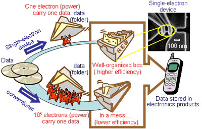
All the world, we can access a huge amount of data and take advantage
of them using various kinds of information technology (IT) supported by
a lot of electronics products, e.g., personal computers, cellular phones,
data servers, and so on. Since an IT society provides us with more useful,
comfortable and friendly life, performance of electronics products has
been continuously improved and numbers of both electronics products and
their users have been increasing. On the other hand, such a trend gives
rise to the serious issue: power consumption to use IT has been also increasing
drastically. The goal of our research is reduction in power consumption
of electronics products. For example, in a transistor, which is one of
the well-known and widely-used devices in electronics products, one information
data is represented by a lot of electrons, which are source of electric
power. What a waste of electrons or power. Our approach to reduce power
consumption is the ultimate reduction of electros representing one information
data: SINGLE ELECTRON.
Single electrons can be treated by various kinds of nanoscale devices
called "single-electron devices (SEDs)". Before the introduction
of such devices, let me explain a metal-oxide-semiconductor field-effect
transistor (MOSFET) which is one of the most used devices and integrated
into an electrical circuit, e.g., CPUs and micro- processors. The MOSFET
has two conductive electrodes, i.e., source and drain, semi- conductor
area (channel) between the electrodes, and gate. There is an insulator
layer between the channel and gate, which means a capacitor. Since the
semiconductor channel is insulative for electrons, there is no current
between the source and drain, which corresponds to an “OFF” state of the
MOSFET. When positive voltage is applied to the gate, negative charges,
i.e., electrons, are induced from the source and the channel becomes conductive.
As a result, electrons can travel from the source and drain, that’s, current
flows through the channel, which corresponds to an “ON” state of the MOSFET.
As easily expected from the case of capacitor, at the ON state, a lot of
electrons are induced randomly and widely in the channel, which prevent
us from dealing with single electrons.
Such difficulty of control of a single electron can be available
in the SEDs. One of the SEDs is a single-electron box (SEB), which is the
most basic one. The SEB has a quite small conductive island, source, and
gate. What’s important here is that the island is extremely small so that
charging energy caused by one electron injected into the island is larger
than thermal energy. Another important thing is that the island is located
close to the source so that electrons can travel between the island and
source owing to tunnel event. These features prevent electrons from entering
the island by thermal energy. This phenomenon is called “Coulomb blockade”
(Proc. IEEE, vol. 87, p. 606-632, 1999). When positive voltage corresponding to the charging energy is applied
to the gate, just one electron can enter the island from the source. The
number of electrons in the island as a function of the gate voltage shows
a staircase pattern. The size of the island in which Coulomb blockade is
active at room temperature is <10 nm.The SEB can be used for a memory
device in which one stored bit is represented by one electron (e.g., Appl. Phys. Lett.v. 68, p. 1377,1996).
Another well-known SED is a single-electron transistor (SET), which
has a source, drain, gate, and island. Although there are gaps between
the drain/source and island, electrons can travel between the source and
drain due to tunneling event. In this case, Coulomb blockade causes interesting
electron tunneling characteristics: when voltage applied to the gate is
changed, current flowing through the SET oscillates uniformly against voltage,
which is called Coulomb blockade oscillation. When voltage is small, no
electron go through the island, that’s, no current flow. When voltage becomes
a value corresponding to the charging energy, single electrons can go through
the island, that’s, current flows. When voltage becomes larger, just one
electron stay at the island and other electrons cannot go through the island
due to Coulomb blockade. These phenomena cause oscillating current characteristics,
which gives new functionality to SET-based circuit (e.g., Tech. Dig. -Int. Electron Devices Meet. (2001) p. 147). The difficulty of realization of SET circuits is to form an extremely
small island (<10 nm) with high quality and controllability. Our group
was succeeded in a development of a unique fabrication method originating
from that of silicon MOSFETs (Tech. Dig. -Int. Electron Devices Meet. (1994) p. 938) and in various kinds of circuit demonstrations.
In the SETs, single electrons go through the island one after another
with random interval. In other wards, it is impossible to transfer one
electron with intended timing. One-by-one electron transfer with precise
timing can be achieved by using single-electron turnstile (Phys. Rev. Lett. V. 64, p. 2691 1990) and pump (Physica B v. 169, p. 573, 1991). Especially, the turnstile composed of an electrically formed island
instead of a physically formed one makes it easy to realize the one-by-one
single-electron transfer with precise timing (Phys. Rev. Lett. v. 67, p. 1626, 1991). This can be achieved by connecting two MOSFETs in series (Appl. Phys. Lett. v. 84, p. 323, 2004). When a MOSFET connected to a source is ON, electrons can flow into the
MOSFET. Then, when two MOSFETs become OFF, one electron can stay at the
center between two MOSFETs due to Coulomb blockade. Next, when the other
MOSFET becomes ON, the electron go into the drain. By repeating such alternative
switching of two MOSFET, single electrons can be transferred with precise
timing, which allows a data information circuit using one electron as one
bit of information (e.g., Appl. Phys. Lett. v. 88, p. 183101, 2006).
 All the world, we can access a huge amount of data and take advantage
of them using various kinds of information technology (IT) supported by
a lot of electronics products, e.g., personal computers, cellular phones,
data servers, and so on. Since an IT society provides us with more useful,
comfortable and friendly life, performance of electronics products has
been continuously improved and numbers of both electronics products and
their users have been increasing. On the other hand, such a trend gives
rise to the serious issue: power consumption to use IT has been also increasing
drastically. The goal of our research is reduction in power consumption
of electronics products. For example, in a transistor, which is one of
the well-known and widely-used devices in electronics products, one information
data is represented by a lot of electrons, which are source of electric
power. What a waste of electrons or power. Our approach to reduce power
consumption is the ultimate reduction of electros representing one information
data: SINGLE ELECTRON.
All the world, we can access a huge amount of data and take advantage
of them using various kinds of information technology (IT) supported by
a lot of electronics products, e.g., personal computers, cellular phones,
data servers, and so on. Since an IT society provides us with more useful,
comfortable and friendly life, performance of electronics products has
been continuously improved and numbers of both electronics products and
their users have been increasing. On the other hand, such a trend gives
rise to the serious issue: power consumption to use IT has been also increasing
drastically. The goal of our research is reduction in power consumption
of electronics products. For example, in a transistor, which is one of
the well-known and widely-used devices in electronics products, one information
data is represented by a lot of electrons, which are source of electric
power. What a waste of electrons or power. Our approach to reduce power
consumption is the ultimate reduction of electros representing one information
data: SINGLE ELECTRON.