| |
Nanodevice's group Advanced Applied Physical Science Laboratory NTT Basic Research Laboratories |
| |
Nanodevice's group Advanced Applied Physical Science Laboratory NTT Basic Research Laboratories |
| Effective Medium Approximation for Variable-Range Hopping | |||
| J. Phys. Soc. Jpn. vol. 94, p. 044001 (2025) DOI: 10.7566/JPSJ.94.044001 | |||
| T. Hayashi, Y. Tokura, and K. Nishiguchi | |||
| [ABSTRACT] The effective medium approximation is extended to include variable-range hopping transport. Homogeneous pair conductances are assigned not only to nearest-neighbor pairs of sites but also to pairs of remote sites. The conductance through a random resistor network is calculated on the basis of both rate equations and the extended effective medium approximation. By comparing their results, it is deduced that the development of long-range ordering in the spatial distribution of voltage potentials is necessary to observe variable-range hopping transport. | |||
| Electron thermometry for Si MOS inversion layer using proximity nano-transistor and its application to Joule-heating experiment | |||
| Appl. Phys. Lett. vol. 126, p. 083501 (2025) DOI: 10.1063/5.0239500 | |||
| H. M. Nayem, M. Hori, K. Nishiguchi, and Y. Ono | |||
| [ABSTRACT] A method for measuring the electron temperature in the inversion layer of Si metal-oxide-semiconductor structures is presented. This technique utilizes a nano-transistor as a thermometer, placed in close proximity to the inversion layer under investigation, enabling measurements of the electron temperature for values above approximately 10 K. When applied to Joule-heating experiments, this method reveals a notable discrepancy between the measurement results and predictions made by the conventional theory based on the deformation-potential coupling with low-energy acoustic phonons. Specifically, the injected-power dependence of the electron temperature is much weaker than expected. The results strongly suggest that another mechanism causing a significant electron energy loss plays a role. | |||
| Ballistic Brownian Motion of Nanoconfined DNA | |||
| ACS Nano vol. 17, 17031-17040 (2023). | |||
| I. Madrid, Z. Zheng, C. Gerbelot, A. Fujiwara, S. Li, S. Grall, K. Nishiguchi, S. H. Kim, A. Chovin, C. Demaille, and N. Clement | |||
| [ABSTRACT] Theoretical treatments of polymer dynamics in liquid generally start with the basic assumption that motion at the smallest scale is heavily overdamped; therefore, inertia can be neglected. We report on the Brownian motion of tethered DNA under nanoconfinement, which was analyzed by molecular dynamics simulation and nanoelectrochemistry-based single-electron shuttle experiments. Our results show a transition into the ballistic Brownian motion regime for short DNA in sub-5 nm gaps, with quality coefficients as high as 2 for double-stranded DNA, an effect mainly attributed to a drastic increase in stiffness. The possibility for DNA to enter the underdamped regime could have profound implications on our understanding of the energetics of biomolecular engines such as the replication machinery, which operates in nanocavities that are a few nanometers wide. | |||
| Single-Cell Electrochemical Aptasensor Array | |||
| ACS Sens. vol. 8, 2921-2926 (2023). | |||
| S. Li, Y. Coffinier, C. Lagadec, F. Cleri, K. Nishiguchi, A. Fujiwara, S. H. Kim, and N. Clement | |||
| [ABSTRACT] Despite several demonstrations of electrochemical devices with limits of detection (LOD) of 1 cell/mL, the implementation of single-cell bioelectrochemical sensor arrays has remained elusive due to the challenges of scaling up. In this study, we show that the recently introduced nanopillar array technology combined with redox-labeled aptamers targeting epithelial cell adhesion molecule (EpCAM) is perfectly suited for such implementation. Combining nanopillar arrays with microwells determined for single cell trapping directly on the sensor surface, single target cells are successfully detected and analyzed. This first implementation of a single-cell electrochemical aptasensor array, based on Brownian-fluctuating redox species, opens new opportunities for large-scale implementation and statistical analysis of early cancer diagnosis and cancer therapy in clinical settings. | |||
| Statistical Properties of Electric Potentials in a Variable-Range Hopping Regime | |||
| J. Phys. Soc. Jpn. vol. 92, p. 034001 (2023). | |||
| T. Hayashi, Y. Tokura, and K. Nishiguchi | |||
| [ABSTRACT] Variable-range hopping transport is studied from a new perspective. Unlike the well-known percolation model for variable-range hopping, which treats the connectivity of bonds between a pair of sites, the emphasis here is on the statistical properties of the voltage potential at these sites. The deviations in the voltage potentials are calculated from the rate equations. The variance and power spectra of the deviations show that there are two temperature regimes: nearest-neighbor hopping at high temperatures and variable-range hopping at low temperatures. The development of long-range order between the voltage deviations in the variable-range hopping regime is confirmed by showing the temperature dependence of the correlation length. | |||
| Subgigahertz Multilayer-Graphene Nanoelectromechanical System Integrated with a Nanometer-Scale Silicon Transistor Driven by Reflectometry | |||
| J. Phys. Soc. Jpn. vol. 92, p. 034001 (2023). | |||
| T. Hayashi, Y. Tokura, and K. Nishiguchi | |||
| [ABSTRACT] We demonstrate the detection of mechanical oscillations of a nanoelectromechanical system (NEMS) composed of a multilayer-graphene (MLG) membrane by using a Si field-effect transistor (FET). The MLG membrane of 500 nm in length is suspended above multiple nanowire channels of the FET functioning as a sensor with high sensitivity. A microwave probe in contact with the FET is connected to double-resonant circuits composed of two inductors and capacitors, and a radio-frequency (rf) signal drives the FET in the resonant condition. When the MLG membrane functioning as a gate of the FET oscillates in mechanical resonance and modulates impedance of the FET, this modulation is monitored using a reflected signal from the resonant circuits. By adjusting the resonant condition using a variable capacitor, the mechanical oscillations of the MLG membrane are detected at 340 MHz. Such rf-signal-driven readout of the NEMS operating at subgigahertz frequency will lead to highly sensitive and functional sensors for small mass and quantum mechanics as well as timing devices. | |||
| CHighly nitrogen-vacancy doped diamond nanostructures fabricated by ion implantation and optimum annealing | |||
| APL Materials vol. 8, p. 031113 (2020). | |||
| H. Sumikura, K. Hirama, K. Nishiguchi, A. Shinya, and M. Notomi | |||
| [ABSTRACT]Nitrogen-vacancy (NV) centers in diamond photonic nanostructures have attracted much attention as efficient single photon emitters and quantum bits. These quantum optical devices mostly require single or low-density NV centers doped in thin diamond membranes. In contrast, this study focuses on diamond photonic nanostructures with a high concentration of NV centers to achieve a diamond color center laser with a sufficient gain available as a visible light source and a sensitive magnetic-field sensor. We employ high-dose helium ion implantation to type-Ib diamond substrates and thermal annealing, which enables us to obtain uniform thin diamond membranes containing a dense ensemble of NV centers. Luminescence spectroscopy reveals the kinetics of NV centers at high temperature from which we find an optimum annealing temperature maximizing the NV center emission while suppressing the transformation from NV to H3 centers. Furthermore, fine photonic nanowires are also successfully fabricated in the air-suspended diamond membrane, and they exhibit intense photoluminescence from the NV centers with a concentration as high as 7 × 1016 cm−3 (0.4 ppm). These results suggest a route to the fabrication of diamond photonic nanostructures containing a dense ensemble of NV centers, which can be a key material for developing diamond-based light emitting and magnetic-field sensing devices. | |||
| Hydrogen Silsesquioxane-Based Nanofluidics | |||
| Adv. Mater. Interfaces vol. 4, p. 1601155 (2017). | |||
| S. Punniyakoti, R. Sivakumarasamy, F. Vaurette, P. Joseph, K. Nishiguchi, A. Fujiwara, and N. Clement | |||
| [ABSTRACT] Nanofluidics show great promise for the control of small volumes and single molecules, especially for biological and energy applications. To build up more and more complex nanofluidics systems, a versatile and reproducible fabrication technique with nanometer precision alignment is desirable. In this article, two e-beam lithography methods to fabricate nanofluidic channels based on hydrogen silsesquioxane, a high-resolution negative-tone inorganic resist, are presented. The robustness and versatility of the fabrication processes are demonstrated on silicon, glass, and flexible substrates. The high precision ability is illustrated with nanometric alignment of nanofluidic channels on gold nanoparticles and nanotransistor sensors, as well as for 3D nanofluidics prototyping. Furthermore, an unexpected extremely slow water evaporation rate (≈1 week for 300 um long nanochannels) is noticed. This feature enables a simple and reliable manipulation of nanofluidic chips for various studies | |||
| An electromechanical displacement transducer | |||
| Appl. Phys. Exp. vol. 9, p. 086701 (2016). | |||
| M. Villiers, I. Mahboob, K. Nishiguchi, D. Hatanaka, A. Fujiwara, and H. Yamaguchi | |||
| [ABSTRACT] Two modes of an electromechanical resonator are coupled through the strain inside the structure with a cooperativity as high as 107, a state-of-the-art value for purely mechanical systems, which enables the observation of normal-mode splitting. This coupling is exploited to transduce the resonator's fundamental mode into the bandwidth of the second flexural mode, which is 1.4 MHz higher in frequency. Thus, an all-mechanical heterodyne detection scheme is implemented that can be developed into a high-precision displacement sensor. | |||
| Observing the semiconducting band-gap alignment of MoS2 layers of different atomic thicknesses using a MoS2/SiO2/Si heterojunction tunnel diode | |||
| Selected for the Featured Article and cover image | |||
| Appl. Phys. Lett. vol. 107, 053101 (2015). | Tunnel diode 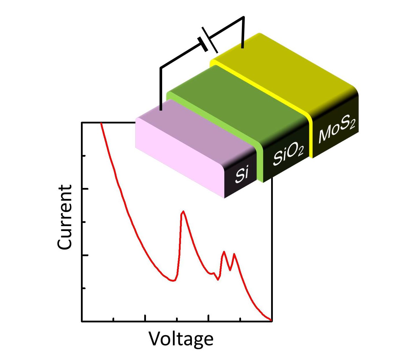 | ||
| K. Nishiguchi, A. Castellanos-Gomez, H. Yamaguchi, A. Fujiwara, H.S. J. van der Zant, G. A. Steele | |||
| [ABSTRACT]We demonstrate a tunnel diode composed of a vertical MoS2/SiO2/Si heterostructure. A MoS2 flake consisting four areas of different thickness functions as a gate terminal of a silicon field-effect transistor. A thin gate oxide allows tunneling current to flow between the n-type MoS2 layers and p-type Si channel. The tunneling-current characteristics show multiple negative differential resistance features, which we interpret as an indication of different conduction-band alignments of the MoS2 layers of different thickness. The presented tunnel device can be also used as a hy-brid-heterostructure device combining the advantages of two-dimensional materials with those of silicon transistors. | |||
| Dispersive and Dissipative Coupling in a Micromechanical Resonator Embedded with a Nanomechanical Resonator | |||
| Nano Letters vol. 15, pp. 2312-2317 (2015). | |||
| I. Mahboob, N. Perrissin , K. Nishiguchi , D. Hatanaka , Y. Okazaki , A. Fujiwara , and H. Yamaguchi | |||
| [ABSTRACT] A micromechanical resonator embedded with a nanomechanical resonator is developed whose dynamics can be captured by the coupled-Van der Pol–Duffing equations. Activating the nanomechanical resonator can dispersively shift the micromechanical resonance by more than 100 times its bandwidth and concurrently increase its energy dissipation rate to the point where it can even be deactivated. The coupled-Van der Pol–Duffing equations also suggest the possibility of self-oscillations. In the limit of strong excitation for the nanomechanical resonator, the dissipation in the micromechanical resonator can not only be reduced, resulting in a quality factor of >3× 10^6, it can even be eliminated entirely resulting in the micromechanical resonator spontaneously vibrating. | |||
| Compact 1D-silicon photonic crystal electro-optic modulator operating with ultra-low switching voltage and energy | |||
| Optics Express vol. 22, pp. 28623-28634 (2014). | |||
| A. Shakoor, K. Nozaki, E. Kuramochi, K. Nishiguchi, A. Shinya, and M. Notomi | |||
| [ABSTRACT] We demonstrate a small foot print (600 nm wide) 1D silicon photonic crystal electro-optic modulator operating with only a 50 mV swing voltage and 0.1 fJ/bit switching energy at GHz speeds, which are the lowest values ever reported for a silicon electro-optic modulator. A 3 dB extinction ratio is demonstrated with an ultra-low 50 mV swing voltage with a total device energy consumption of 42.8 fJ/bit, which is dominated by the state holding energy. The total energy consumption is reduced to 14.65 fJ/bit for a 300 mV swing voltage while still keeping the switching energy at less than 2 fJ/bit. Under optimum voltage conditions, the device operates with a maximum speed of 3 Gbps with 8 dB extinction ratio, which rises to 11 dB for a 1 Gbps modulation speed. | |||
| Electric tuning of direct-indirect optical transitions in silicon | |||
| Sci. Rep. vol. 4, p. 6950 (6 pages) (2014). | |||
| J. Noborisaka, K. Nishiguchi, and A. Fujiwara | |||
| [ABSTRACT] Electronic band structures in semiconductors are uniquely determined by the constituent elements of the lattice. For example, bulk silicon has an indirect bandgap and it prohibits efficient light emission. Here we report the electrical tuning of the direct/indirect band optical transition in an ultrathin silicon-on-insulator (SOI) gated metal-oxide-semiconductor (MOS) light-emitting diode. A special Si/SiO2 interface formed by high-temperature annealing that shows stronger valley coupling enables us to observe phononless direct optical transition. Furthermore, by controlling the gate field, its strength can be electrically tuned to 16 times that of the indirect transition, which is nearly 800 times larger than the weak direct transition in bulk silicon. These results will therefore assist the development of both complementary MOS (CMOS)-compatible silicon photonics and the emerging “valleytronics” based on the control of the valley degree of freedom. | |||
| Multi-mode parametric coupling in an electromechanical resonator | |
| Appl. Phys. Lett. vol. 103, p. 153105 (2013). | |
| I. Mahboob, V. Nier, K. Nishiguchi, A. Fujiwara, and H. Yamaguchi | |
| [ABSTRACT] Parametric coupling between multiple vibration modes in an electromechanical resonator is demonstrated via a strain inducing piezoelectric pump which enables construction of a mechanical-vibration register. In particular, the coupling between the flexural and torsional vibration modes can exceed their intrinsic dissipation rates enabling operation deep into the strong-coupling regime. The dynamic nature of this parametric coupling also permits temporal manipulation of the mechanical-vibration register enabling both long-lived modes to be rapidly switched off and phonon populations to be coherently exchanged between modes. | |
| Water Electrolysis and Energy Harvesting with Zero-Dimensional Ion-Sensitive Field-Effect Transistors | |
| Nano Lett. vol. 13, p. 3903 (2013) | |
| N. Clément, K. Nishiguchi, J. F. Dufreche, D. Guerin, A. Fujiwara, and D. Vuillaume | |
| [ABSTRACT]The relationship of the gas bubble size to the size distribution critically influences the effectiveness of electrochemical processes. Several optical and acoustical techniques have been used to characterize the size and emission frequency of bubbles. Here, we used zero-dimensional (0D) ion-sensitive field-effect transistors (ISFETs) buried under a microbath to detect the emission of individual bubbles electrically and to generate statistics on the bubble emission time. The bubble size was evaluated via a simple model of the electrolytic current. We suggest that energy lost during water electrolysis could be used to generate electric pulses at an optimal efficiency with an array of 0D ISFETs. | |
| Phonon Lasing in an Electromechanical Resonator | |
| Phys. Rev. Lett. vol. 110, p. 127202 (2013) | |
| I. Mahboob, K. Nishiguchi, A. Fujiwara, and H. Yamaguchi | |
| [ABSTRACT]An electromechanical resonator harboring an atomlike spectrum of discrete mechanical vibrations, namely, phonon modes, has been developed. A purely mechanical three-mode system becomes available in the electromechanical atom in which the energy difference of the two higher modes is resonant with a long-lived lower mode. Our measurements reveal that even an incoherent input into the higher mode results in coherent emission in the lower mode that exhibits all the hallmarks of phonon lasing in a process that is reminiscent of Brillouin lasing. | |
| Detecting signals buried in noise via nanowire transistors using stochastic resonance | |||
| Appl. Phys. Lett. vol. 101, p. 193108 (2012). | Signal detection using a transitor with small S-swing 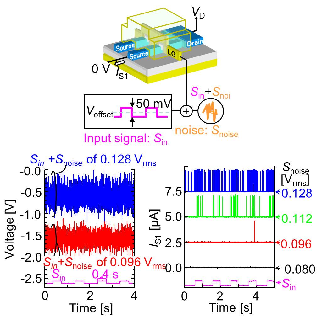 | ||
| K. Nishiguchi and A. Fujiwara | |||
| [ABSTRACT] We demonstrate stochastic resonance (SR), which takes advantage of noise to detect a weak signal, using a field-effect transistor (FET). An FET’s structure composed of a nanowire channel enables current characteristics to show strong nonlinearity, which overcomes thermal limitation, and dynamic bistability, both of which boost an effect of SR and silhouette noise from noise. Moreover, the dynamic bistability enables SR effect to be enhanced by adding common noise to multiple FETs. The FET providing such unique characteristics opens the way to use SR for practical applications. | |||
| Nanowire Metal-Oxide-Semiconductor Field-Effect Transistors with Small Subthreshold | |||
| Appl. Phys. Express, vol. 5, p. 085002 (2012). | Transitor with small S-swing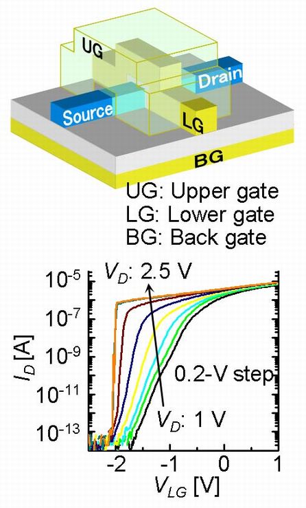 | ||
| K. Nishiguchi and A. Fujiwara | |||
| [ABSTRACT]We demonstrate metal-oxide-semiconductor field-effect transistors (MOSFETs) with small subthreshold swing (SS). The MOSFETs have a nanowire channel and three gates. A parasitic bipolar transistor formed in a fully depleted silicon-on-insulator MOSFET applies body bias to the MOSFET’s channel and thus reduces the SS. Additionally, triple-gate operation makes drain voltage smaller and provides current characteristics with a high on/off ratio and small hysteresis. As a result, SSs of the n-type and p-type MOSFETs reach 6.6 and 5.2 mV/dec, respectively, in the range of current of six orders of magnitude. These features promise MOSFETs with low power consumption. | |||
| Phonon-cavity electromechanics | |
| Nature Physics, vol. 8, pp. 387-392 (2012) | |
| I. Mahboob, K. Nishiguchi, H. Okamoto, and H. Yamaguchi | |
| [ABSTRACT]Photonic cavities have emerged as an indispensable tool to control and manipulate harmonic motion in opto/electromechanical systems. Invariably, in these systems a high-quality-factor photonic mode is parametrically coupled to a high-quality-factor mechanical oscillation mode. This entails the demanding challenges of either combining two physically distinct systems, or else optimizing the same nanostructure for both mechanical and optical properties. In contrast to these approaches, here we show that the cavity can be realized by the second oscillation mode of the same mechanical oscillator. A piezoelectric pump generates strain-induced parametric coupling between the first and the second mode at a rate that can exceed their intrinsic relaxation rate. This leads to a mechanically induced transparency in the second mode which plays the role of the phonon cavity, the emergence of parametric normal-mode splittingand the ability to cool the first mode. Thus, the mechanical oscillator can now be completely manipulated by a phonon cavity | |
| Tuneable electromechanical comb generation | |
| Appl. Phys. Lett. vol. 100, p. 113109 (2012) | |
| I. Mahboob, Q. Wilmart, K. Nishiguchi, A. Fujiwara, and H. Yamaguchi | |
| [ABSTRACT]An array of equally spaced oscillations or a comb is created within the bandwidth of the fundamental mode of an electromechanical resonator. This phenomenon utilises 2 continuous-wave (CW) pump excitations that piezoelectrically modulate the tension in the mechanical element and is seeded by a CW harmonic excitation of the first mode i.e., the signal. The resultant comb can be dynamically manipulated via the pumps and signal where the teeth separation can be tuned over 3 orders of magnitude and the comb density can be increased from just 2 teeth to nearly 10^2. (c) 2012 American Institute of Physics | |
| Bound exciton photoluminescence from ion-implanted phosphorus in thin silicon layers | |
| Optics Express, vol. 19, p. 25255 (2011). | |
| H. Sumikura, K. Nishiguchi, Y. Ono, A. Fujiwara, and M. Notomi | |
| [ABSTRACT]We report the observation of clear bound exciton (BE) emission from ion-implanted phosphorus. Shallow implantation and high-temperature annealing successfully introduce active donors into thin silicon layers. The BE emission at a wavelength of 1079 nm shows that a part of the implanted donors are definitely activated and isolated from each other. However, photoluminescence and electron spin resonance studies find a cluster state of the activated donors. The BE emission is suppressed by this cluster state rather than the nonradiative processes caused by ion implantation. Our results provide important information about ion implantation for doping quantum devices with phosphorus quantum bits. (c) 2011 OSA | |
| Wide-band idler generation in a GaAs electromechanical resonator | |
| Phys. Rev. B, vol. 84, p. 113411 (2011). | |
| I. Mahboob, Q. Wilmart, K. Nishiguchi, A. Fujiwara, and H. Yamaguchi | |
| [ABSTRACT]Periodically modulating the piezoelectrically introduced strain in an electromechanical resonator can enable the fundamental (ω0) and the first modes (ω1) to be coupled. This is explicitly demonstrated with the creation of a mechanical idler at ω1 (ω0) when a signal excitation is applied at ω0 (ω1) and a pump excitation is applied at ω0+ω1. The dynamics of the mechanical idler generation are captured by a simple phenomenological model and our experimental demonstration paves the way toward accessing the diverse functionality of nonlinear optics in an on-chip electromechanical platform. | |
| Large Array of Sub-10-nm Single-Grain Au Nanodots for use in Nanotechnology | |
| Small, DOI: 10.1002/smll.201100915 (2011). | |
| N. Clement, G. Patriarche, K. Smaali, F. Vaurette, K. Nishiguchi, D. Troadec, A. Fujiwara, D. Vuillaume | |
| [ABSTRACT]A uniform array of single-grain Au nanodots, as small as 5--8 nm, can be formed on silicon using e-beam lithography. The as-fabricated nanodots are amorphous, and thermal annealing converts them to pure Au single crystals covered with a thin SiO2 layer. These findings are based on physical measurements, such as atomic force microscopy (AFM), atomic-resolution scanning transmission electron microscopy, and chemical techniques using energy dispersive X-ray spectroscopy. A self-assembled organic monolayer is grafted on the nanodots and characterized chemically with nanometric lateral resolution. The extended uniform array of nanodots is used as a new test-bed for molecular electronic devices. | |
| Strong Stark effect in electroluminescence from phosphorous-doped silicon-on-insulator metal-oxide-semiconductor field-effect transistors | |||
| Appl. Phys. Lett., vol. 98, p. 033503 (2011). | |||
| J. Noborisaka, K. Nishiguchi, Y. Ono, H. Kageshima, and A. Fujiwara | |||
| [ABSTRACT] We report a strong Stark effect in electroluminescence (EL) from thin silicon-on-insulator metal-oxide-semiconductor field-effect transistors. The EL peak shows a large Stark shift of up to 50 meV when a gate-induced electric field is applied. Such a large shift is observed because of the strong confinement of carriers by a Si/SiO2 quantum well. Furthermore, we observe a sudden decrease of EL intensity at a specific electric field. This feature is ascribed to electron dissociation from phosphorous atom to subbands in a triangular well at the Si/SiO2 interface by the applied electric field. c 2011 American Institute of Physics | |||
| Interconnect-free parallel logic circuits in a single mechanical resonator | |||
| Nature Communications, v. 2, DOI:10.1038/ncomms1201 (2011). | |||
| I. Mahboob, E. Flurin, K. Nishiguchi, A. Fujiwara, and H. Yamaguchi | |||
| [ABSTRACT] In conventional computers, wiring between transistors is required to enable the execution of Boolean logic functions. This has resulted in processors in which billions of transistors are physically interconnected, which limits integration densities, gives rise to huge power consumption and restricts processing speeds. A method to eliminate wiring amongst transistors by condensing Boolean logic into a single active element is thus highly desirable. Here, we demonstrate a novel logic architecture using only a single electromechanical parametric resonator into which multiple channels of binary information are encoded as mechanical oscillations at different frequencies. The parametric resonator can mix these channels, resulting in new mechanical oscillation states that enable the construction of AND, OR and XOR logic gates as well as multibit logic circuits. Moreover, the mechanical logic gates and circuits can be executed simultaneously, giving rise to the prospect of a parallel logic processor in just a single mechanical resonator. | |||
| Enhanced force sensitivity and noise squeezing in an electromechanical resonator coupled to a nanotransistor | |||
| Appl. Phys. Lett., vol. 97, p. 253105 (2010). | |||
| I. Mahboob, E. Flurin, K. Nishiguchi, A. Fujiwara, and H. Yamaguchi | |||
| [ABSTRACT] A nanofield-effect transistor (nano-FET) is coupled to a massive piezoelectricity based electromechanical resonator integrated with a parametric amplifier. The mechanical parametric amplifier can enhance the resonator’s displacement and the resulting electrical signal is further amplified by the nano-FET. This hybrid amplification scheme yields an increase in the mechanical displacement signal by 70 dB resulting in a force sensitivity of 200 aNHz^-1/2 at 3 K. The mechanical parametric amplifier can also squeeze the displacement noise in one oscillation phase by 5 dB enabling a factor of 4 reduction in the thermomechanical noise force level. c 2010 American Institute of Physics | |||
| Separately contacted monocrystalline silicon double-layer structure with an amorphous silicon dioxide barrier made by wafer bonding | |||
| Semiconductor Science and Technology, vol. 25, p. 125001 (2010) | |||
| K. Takashina, M. Nagase, K. Nishiguchi, Y. Ono, H. Omi, A. Fujiwara, T. Fujisawa, and K. Muraki | |||
| [ABSTRACT] A double layer of monocrystalline silicon separated by a 23.5 nm silicon dioxide barrier is fabricated by bonding two silicon-on-insulator wafers with oxidized surface layers. The two layers are separately contacted allowing transport measurements through individual layers and a bias voltage to be applied between the layers. Four-terminal magnetotransport measurements at cryogenic temperatures on electrons generated close to the central oxide barrier show reasonable mobility. | |||
| Tunneling spectroscopy of electron subbands in thin silicon-on-insulator metal-oxide-semiconductor field-effect transistors | |||
| Appl. Phys. Lett., vol. 96, p. 112102 (2010). | |||
| J. Noborisaka, K. Nishiguchi, H. Kageshima, Y. Ono, and A. Fujiwara | |||
| [ABSTRACT] We report the tunneling spectroscopy of thin silicon-on-insulator (SOI) metal-oxide-semiconductor field-effect transistors with tunneling gate oxide. When electrons are injected into a thin SOI well, the gate-tunneling current shows kink structures originating from quantized energy levels in the SOI well. From the theoretical consideration of the energy levels and their density of states, the observed features can be ascribed to electron tunneling into the in-plane fourfold degenerate valley subbands. Furthermore, inhomogeneous peak broadening of the kink structures in the experiment is well explained by the SOI thickness variation. c 2010 American Institute of Physics | |||
| Room temperature piezoelectric displacement detection via a silicon field effect transistor | |||
| Appl. Phys. Lett., vol. 95, p. 233102 (2009). | |||
| I. Mahboob, K. Nishiguchi, A. Fujiwara, and H. Yamaguchi | |||
| [ABSTRACT] An electromechanical oscillator embedded with a two dimensional electron gas is capacitively coupled to a silicon field effect transistor (Si-FET). The piezovoltage induced by the mechanical motion modulates the current passing through the Si-FET enabling the electromechanical oscillator’s position to be monitored. When the Si-FET is biased at its optimal point, the motion induced piezovoltage can be amplified resulting in a displacement sensitivity of 6×10^-12 mHz^-1/2 for a 131 kHz GaAs resonator which is among the highest recorded for an all-electrical room temperature detection scheme. c 2009 American Institute of Physics | |||
| Low power and fast electro-optic silicon modulator with lateral p-i-n embedded photonic crystal nanocavity | |||
| Optics Express, vol. 17, 22505-22513 (2009) | |||
| T. Tanabe, K. Nishiguchi, E. Kuramochi, and M. Notomi | |||
| [ABSTRACT] We have fabricated high-Q photonic crystal nanocavities with a lateral p-i-n structure to demonstrate low-power and high-speed electro-optic modulation in a silicon chip. GHz operation is demonstrated at a very low (μW level) operating power, which is about 4.6 times lower than that reported for other cavities in silicon. This low-power operation is due to the small size and high-Q of the photonic crystal nanocavity. c 2009 OSA | |||
| Horizontal position analysis of single acceptors in Si nanoscale field-effect transistors | |||
| Appl. Phys. Lett., vol. 94, 223501 (2009) | |||
| M. A. H. Khalafalla, Y. Ono, K. Nishiguchi, and A. Fujiwara | |||
| [ABSTRACT] The authors performed conductance measurements to identify the horizontal position of single boron acceptors in silicon-on-insulator nanoscale field-effect transistors at a temperature of 6 K. The horizontal position, i.e., how far the acceptor is from the source or drain terminal, is qualitatively obtained, and it is shown, on the level of single dopants, that the acceptor near the source significantly affects the subthreshold nature of the transistor. c 2009 American Institute of Physics | |||
| Electrons and holes in a 40 nm thick silicon slab at cryogenic temperatures | |||
| Appl. Phys. Lett., vol. 94, 142104 (2009) | |||
| K. Takashina, K. Nishiguchi, Y. Ono, A. Fujiwara, T. Fujisawa, Y. Hirayama, and K. Muraki | |||
| [ABSTRACT] We demonstrate low temperature operation of an electron-hole bilayer device based on a 40 nm thick layer of silicon in which electrons and holes can be simultaneously induced and contacted independently. The device allows the application of bias between the electrons and holes enhancing controllability over density and confining potential. We confirm that drag measurements are possible with the structure. c 2009 American Institute of Physics | |||
| Low-energy electron emission from an electron inversion layer of a Si/SiO2/Si cathode for nano-decomposition | |||
| Jpn. J. Appl. Phys., vol. 47, pp. 5106-5108 (2008). | Electron emission from mos structure 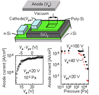 | ||
| K. Nishiguchi, M. Nagase, T. Yamaguchi, A. Fujiwara, and H. Yamaguchi | |||
| [ABSTRACT] We fabricated an electron-emission cathode with a Si/SiO2/Si structure using metal-oxide-semiconductor field-effect transistor (MOSFET) fabrication technology. Electrons travel from an electron-source Si layer to a thin polycrystalline Si (poly-Si) through a thin SiO2 and some of them with high energy, i.e., hot electrons, are emitted from the poly-Si surface. By utilizing an electron-inversion layer as the electron source, high efficiency and stability of electron emission were achieved. Material decomposition at a depth of a few nanometers was also demonstrated using a low-energy-electron irradiation from the cathode operated in a low vacuum condition. | |||
| Long retention of gain-cell dynamic random-access memory with undoped memory node | |||
| IEEE Electron Device Lett. vol. 28, pp. 48-50 (2007). | Memory operation with long retention  | ||
| K. Nishiguchi, A. Fujiwara, Y. Ono, H. Inokawa, and Y. Takahashi | |||
| [ABSTRACT] Low current leakage characteristics of a novel silicon-on-insulator (SOI) device are investigated in view of application to a gain-cell dynamic random access memory (DRAM). The device consists of a two-layered poly-Si gate. Since, in this device, the memory node is electrically formed by the gate in undoped SOI wire, no p-n junction is required. The retention is found to be dominated by the subthreshold leakage, which leads to long data retention. The device also achieved a fast (10 ns) writing time and its fabrication process is compatible with those of SOI MOSFETs. The present results, thus, strongly suggest a way of conducting a gain-cell DRAM to be embedded into logic circuits. | |||
| Fast All-Optical Switching using Ion-Implanted Silicon Photonic Crystal Nanocavities | |||
| Appl. Phys. Lett., vol. 90, 031115 (2007) | |||
| T. Tanabe, K. Nishiguchi, A. Shinya, E. Kuramochi, H. Inokawa, and M. Notomi | |||
| [ABSTRACT] On-chip all-optical switching based on the carrier plasma dispersion in an argon ion (Ar+) implanted photonic crystal (PhC) nanocavity that is connected to input/output waveguides is described. A high dose of Ar+ is introduced, and annealing is used to recrystallize the silicon and thus create dislocation loops at the center of the PhC slab. Dislocation loops enable the fast recombination of the carriers, which allows a fast switching recovery time for PhC switches. The switching window is threehr times smaller than that without ion implantation, while the required operating energy remains almost the same (<100 fJ). c 2007 American Instituteu of Physics | |||
| Impurity conduction in phosphorus-doped buried-channel silicon-on-insulator field-effect transistors at temperatures between 10 and 295 K | |||
| Phys. Rev. B, vol. 74, p. 235317 (2006) | |||
| Y. Ono, J-F Morizur, K. Nishiguchi, K. Takashina, and H. Yamaguchi | |||
| [ABSTRACT] Received 27 July 2006; revised 21 October 2006; published 14 December 2006 We investigate transport in phosphorus-doped buried-channel metal-oxide-semiconductor field-effect transistors at temperatures between 10 and 295 K. We focus on transistors with phosphorus donor concentrations higher than those previously studied, where we expect conduction to rely on donor electrons rather than conduction-band electrons. In a range of doping concentration between around 2.1 and 8.7×10^17 cm^-3, we find that a clear peak emerges in the conductance versus gate-voltage curves at low temperature. In addition, temperature dependence measurements reveal that the conductance obeys a variable-range-hopping law up to an unexpectedly high temperature of over 100 K. The symmetric dual-gate configuration of the silicon-on-insulator we use allows us to fully characterize the vertical-bias dependence of the conductance. Comparison to computer simulation of the phosphorus impurity band depth profile reveals how the spatial variation of the impurity-band energy determines the hopping conduction in transistor structures. We conclude that the emergence of the conductance peak and the high-temperature variable-range hopping originate from the band bending and its change by the gate bias. Moreover, the peak structure is found to be strongly related to the density of states (DOS) of the phosphorus impurity band, suggesting the possibility of performing a spectroscopy for the DOS of phosphorus, the dopant of paramount importance in Si technology, through transport experiments. c 2006 The American Physical Society | |||
| Ballistic Transport in Silicon Nanostructure | |
| Silicon Nanoelectronics ed S. Oda and D. Ferry (Marcel Dekker Inc), p.105 (2005). | |
| H. Mizuta, K. Nishiguchi, and S. Oda | |
| Charge-state control of phosphorous donors in silicon-on-insulator metal-oxide-semiconductor field-effect transistor | |||
| Jpn. J. Appl. Phys., vol. 44, p. 2588 (2005). | |||
| Y. Ono, A. Fujiwara, K. Nishiguchi, H. Inokawa, and Y. Takahashi | |||
| [ABSTRACT] The drain current vs gate-voltage characteristics of a phosphorus-doped n-channel silicon-on-insulator metal-oxide-semiconductor field-effect transistor have been investigated. It was shown that, by controlling the voltage to the substrate at 20 K, the charge states of phosphorus donors can be changed in a controlled manner. Most of the donors are neutralized for the substrate voltage of around 0 V, while a major portion of the donors is ionized for a positive or negative voltage. Such a change can be detected by monitoring the change in the threshold voltage of the transistor. This is an experimental demonstration of the systematic control and monitoring of donor charge states in silicon. | |||
| Nanocrystalline silicon electron emitter with a high efficiency enhanced by a planarization technique | |||
| J. Appl. Phys., vol. 92, pp. 2748-2757 (2002). | |||
| K. Nishiguchi, X. Zhao and S. Oda | |||
| [ABSTRACT] A cold electron emitter has been fabricated based on nanocrystalline silicon (nc-Si) quantum dots formed in the gas phase by very-high-frequency plasma decomposition of SiH4. A small size of less than 10 nm and the spherical shape of the nc-Si dots facilitated the generation of hot electrons. Electrons with kinetic energies higher than the work function of the top electrode were extracted into vacuum through the electrode. A planarization process of the nc-Si layer by annealing enhanced the electron emission efficiency to 5%. Efficiency was optimized by varying the thicknesses of the nc-Si layer, the SiO2 layer, and the top electrode film. c 2002 American Institute of Physics. | |||
| Ballistic transport in silicon vertical transistors | |||
| J. Appl. Phys., vol. 92, pp. 1399-1405 (2002). | |||
| K. Nishiguchi and S. Oda | |||
| [ABSTRACT] Clear evidence for ballistic transport has been observed at 5 K from silicon vertical transistors with wrap around gates. The effect of channel shape was investigated experimentally and accounted for theoretically by the anisotropy of the Si conduction band. A reduction in conductance and the appearance of multiple steps were observed when a magnetic field was applied perpendicular to the channel. These results were successfully modeled within the effective mass approximation by including the magnetic vector potential and effects due to series resistance and the spin and valley degeneracy. c 2002 American Institute of Physics. | |||
| A self-aligned two-gate single-electron transistor derived from 0.12μm lithography | |||
| Appl. Phys. Lett., vol. 78, pp. 2070-2072 (2001). | |||
| K. Nishiguchi and S. Oda | |||
| [ABSTRACT] A single-electron transistor (SET) with two gates was fabricated via the self-aligned evaporation of Al into a trench structure comprised of Si and SiO2. The initial trench, which was comparable to 0.12 μm lines and defined by electron-beam lithography, was reduced to 0.05×0.02 μm by a slightly anisotropic etching characteristic. These processes allow for the production of SET devices using current silicon fabrication techniques. The simultaneous formation of two gates allows for one gate to be used to control the background charge of each device. The shift of Coulomb oscillation peaks was clearly shown by controlling the second gate bias. An inverter logic operation at a temperature of 5 K with a gain of 1.3 was obtained. These characteristics indicate that such SET logic devices, based on a combination of the good performance of the Al SET and the high level of control of the fabrication of Si technology, have considerable potential for future use. c 2001 American Institute of Physics. | |||
| Electron transport in a single silicon quantum structure using a vertical silicon probe | |||
| J. Appl. Phys., vol. 88, pp. 4186-4190 (2000). | |||
| K. Nishiguchi and S. Oda | |||
| [ABSTRACT] We present a method of electrical measurement of single nanocrystalline silicon (nc-Si) particles fabricated by plasma-enhanced chemical vapor deposition (CVD) at very high frequency of 144 MHz. A vertical Si probe structure with a spheroidal shaped hole in SiO2 and a CVD grown polycrystalline Si electrode allows stable measurement of current through a single nc-Si quantum dot. Periodic Coulomb staircases are observed between 5 and 50 K. The temperature dependence of the differential conductance is consistent with these being electron transport through a double junction array. A Monte Carlo simulation further supports the double junction array model where a nc-Si quantum dot is covered by 1.5-nm-thick natural oxide as a tunnel barrier. Moreover, applying a wraparound gate makes it possible to observe Coulomb oscillation. c 2000 American Institute of Physics. | |||
| Conductance quantization in nanoscale vertical-structure silicon field-effect transistors with a wrap gate | |||
| Appl. Phys. Lett, vol. 76, pp. 2922-2924 (2000) | |||
| K. Nishiguchi and S. Oda | |||
| [ABSTRACT] Experimental results of quantum ballistic transport in single quantum contact by using vertical structure silicon field effect transistors with a wrap gate are presented. Based on dc measurement, the conductance」oltage characteristics show quantized plateaus at multiples of 2e^2/h. The devices were prepared by electron beam lithography and by combinations of various types of etching. The channel is fabricated by the chemical vapor deposition of amorphous silicon and solid-phase crystallization. The vertical structure allows a channel length as short as 30 nm, which is defined by the film thickness. The effective channel is reduced by the depletion potential, resulting in a much narrower channel width compared to the geometrical width of 60 nm. Thus, the effective size of the silicon transistor is smaller than the elastic mean free path of 40 nm, resulting in the conduction quantization at 3-5 K. c 2000 American Institute of Physics. | |||