| |
Nanodevice's group Advanced Applied Physical Science Laboratory NTT Basic Research Laboratories |
| |
Nanodevice's group Advanced Applied Physical Science Laboratory NTT Basic Research Laboratories |
| Subgigahertz Multilayer-Graphene Nanoelectromechanical System Integrated with a Nanometer-Scale Silicon Transistor Driven by Reflectometry | |||
| Phys. Rev. Applied vol. 19, p. L011003 (2023). | |||
| K. Nishiguchi, H. Yamaguchi, and A. Fujiwara | |||
| [ABSTRACT] We demonstrate the detection of mechanical oscillations of a nanoelectromechanical system (NEMS) composed of a multilayer-graphene (MLG) membrane by using a Si field-effect transistor (FET). The MLG membrane of 500 nm in length is suspended above multiple nanowire channels of the FET functioning as a sensor with high sensitivity. A microwave probe in contact with the FET is connected to double-resonant circuits composed of two inductors and capacitors, and a radio-frequency (rf) signal drives the FET in the resonant condition. When the MLG membrane functioning as a gate of the FET oscillates in mechanical resonance and modulates impedance of the FET, this modulation is monitored using a reflected signal from the resonant circuits. By adjusting the resonant condition using a variable capacitor, the mechanical oscillations of the MLG membrane are detected at 340 MHz. Such rf-signal-driven readout of the NEMS operating at subgigahertz frequency will lead to highly sensitive and functional sensors for small mass and quantum mechanics as well as timing devices. | |||
| Room-temperature several-hundred-of-megahertz charge sensing with single-electron resolution using a silicon transistor | |||
| Appl. Phys. Lett. vol. 122, p. 043502 (2023). | |||
| K. Nishiguchi, H. Yamaguchi, A. Fujiwara, H. S. J. van der Zant, and G.A. Steele | |||
| [ABSTRACT] We demonstrate charge detection with single-electron resolution at high readout frequency using a silicon field-effect transistor (FET) integrated with double resonant circuits. A FET, whose channel of 10-nm width enables a single electron to be detected at room temperature, is connected to resonant circuits composed of coupled inductors and capacitors, and these double resonant circuits provide two resonance frequencies. When the FET is driven by a carrier signal at the lower resonance frequency, a small signal applied to the FET's gate modulates the resonance condition, resulting in a reflected signal appearing near the higher resonance frequency. Such operation utilizing the double resonant circuits enables charge detection with a single-electron resolution of 3 × 10⁻³ e/Hz0.5 and a readout frequency of 200 MHz at room temperature. In addition, a variable capacitor used in the double resonant circuits allows charge-sensing characteristics to be controlled in situ. | |||
| Redox-labelled electrochemical aptasensors with nanosupported cancer cells | |||
| Biosensors and Bioelectronics vol. 216, p. 114643 (2022). | |||
| S.Li, C.Lagadec, F.Cleri, K.Nishiguchi, A.Fujiwara, T.Fujii, S.-H.Kim, and N.Clément | |||
| [ABSTRACT] The transfer of redox-labelled bioelectrochemical sensors from proteins to cells is not straightforward because of the cell downward force issue on the surface of the sensors. In this paper, 20-nm-thick nanopillars are introduced to overcome this issue, in a well-controlled manner. We show on both molecular dynamics simulations and experiments that suspending cells a few nanometers above an electrode surface enables redox-labelled tethered DNA aptamer probes to move freely, while remaining at an interaction distance from a target membrane protein, i. e. epithelial cell adhesion molecule (EpCAM), which is typically overexpressed in cancer cells. By this nanopillar configuration, the interaction of aptamer with cancer cells is clearly observable, with 13 cells as the lower limit of detection. Nanoconfinement induced by the gap between the electrode surface and the cell membrane appears to improve the limit of detection and to lower the melting temperature of DNA aptamer hairpins, offering an additional degree of freedom to optimize molecular recognition mechanisms. This novel nanosupported electrochemical DNA cell sensor scheme including Brownian-fluctuating redox species opens new opportunities for the design of all-electrical sensors using redox-labelled probes. | |||
| Seebeck effect in a nanometer-scale dot in a Si nanowire observed with electron counting statistics | |||
| Selected for Cover Art | |||
| Appl. Phys. Lett. vol. 121, p. 183501 (2022). | |||
| K. Chida, A. Fujiwara, and K. Nishiguchi | |||
| [ABSTRACT] We performed electron counting statistics to measure the thermoelectric effect in a nanometer-scale silicon dot. To separate the 100-nm-long dot from a silicon nanowire, we used an electrostatically created 30-nm-long energy barrier. By measuring current through a nearby sensor, we observed the random motion of single electrons between the dot and silicon nanowire. The statistics of single-electron motion provides us with information on temperature and voltage at the dot. Under the detailed balance assumption, we determined the temperature difference and the Seebeck voltage between the dot and silicon nanowire. The validity of our analysis was confirmed by observing the energy-barrier height dependence of the Seebeck coefficient. Furthermore, by counting the electrons leaving the dot, a minute output power on the order of sub-zeptowatt from the dot to the silicon nanowire was estimated. | |||
| Selective layer-free blood serum ionogram based on ion-specific interactions with a nanotransistor | |||
| Nature Mater. vol. 17, pp. 464-470 (2018). | |||
| R. Sivakumarasamy, R. Hartkamp, B. Siboulet, J. -F. Dufreche, K. Nishiguchi, A. Fujiwara, and N. Clement | |||
| [ABSTRACT] Despite being ubiquitous in the fields of chemistry and biology, the ion-specific effects of electrolytes pose major challenges for researchers. A lack of understanding about ion-specific surface interactions has hampered the development and application of materials for (bio-) chemical sensor applications. Here, we show that scaling a silicon nanotransistor sensor down to similar to 25 nm provides a unique opportunity to understand and exploit ion-specific surface interactions, yielding a surface that is highly sensitive to cations and inert to pH. The unprecedented sensitivity of these devices to Na+ and divalent ions can be attributed to an overscreening effect via molecular dynamics. The surface potential of multi-ion solutions is well described by the sum of the electrochemical potentials of each cation, enabling selective measurements of a target ion concentration without requiring a selective organic layer. We use these features to construct a blood serum ionogram for Na+, K+, Ca2+ and Mg2+, in an important step towards the development of a versatile, durable and mobile chemical or blood diagnostic tool. | |||
| Hydrogen Silsesquioxane-Based Nanofluidics | |||
| Adv. Mater. Interfaces vol. 4, p. 1601155 (2017). | |||
| S. Punniyakoti, R. Sivakumarasamy, F. Vaurette, P. Joseph, K. Nishiguchi, A. Fujiwara, and N. Clement | |||
| [ABSTRACT] Nanofluidics show great promise for the control of small volumes and single molecules, especially for biological and energy applications. To build up more and more complex nanofluidics systems, a versatile and reproducible fabrication technique with nanometer precision alignment is desirable. In this article, two e-beam lithography methods to fabricate nanofluidic channels based on hydrogen silsesquioxane, a high-resolution negative-tone inorganic resist, are presented. The robustness and versatility of the fabrication processes are demonstrated on silicon, glass, and flexible substrates. The high precision ability is illustrated with nanometric alignment of nanofluidic channels on gold nanoparticles and nanotransistor sensors, as well as for 3D nanofluidics prototyping. Furthermore, an unexpected extremely slow water evaporation rate (≈1 week for 300 um long nanochannels) is noticed. This feature enables a simple and reliable manipulation of nanofluidic chips for various studies | |||
| A correlated electromechanical system | |||
| New J. Phys. vol. 19, p. 033026 (2017). | |||
| I. Mahboob, M. Villiers, K. Nishiguchi, D. Hatanaka, A. Fujiwara, and H. Yamaguchi | |||
| [ABSTRACT]A correlation with phonons sustained by a pair of electromechanical resonators that differ both in size and frequency is demonstrated. In spite of the electromechanical resonators being spatially distinct, they can still be strongly dynamically coupled via a classical analogue of the beam splitter interaction with a cooperativity exceeding five, and parametric down-conversion which results in both resonators self-oscillating. This latter regime yields a classical variant of a two-mode squeezed state which is identified as perfectly correlated phase-locked vibrations between the two resonators. The creation of a correlation between two separate mechanical resonators suggests that extending this interaction to vacuum phonon states could enable a macroscopic two-mode squeezed state to be generated. Conversely, the ability to resolve the correlated state via the self-oscillations could be harnessed to build a new class of detector where an external stimulus neutralises the phase-locked vibrations. | |||
| Single-electron thermal noise | |||
|
Picked up in LAB TALK of nanotechweb.org and Nanotechnology. Picked up in IOPselect. | |||
| Nanotechnology vol. 25, p. 275201 (2014). | Single-electron detection of thermal noise 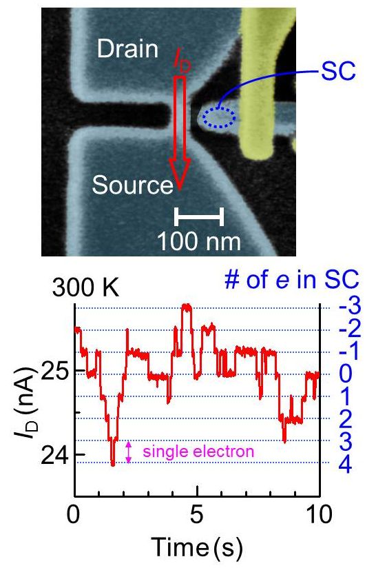 | ||
| K. Nishiguchi, Y. Ono, and A. Fujiwara | |||
| [ABSTRACT] We report the observation of thermal noise on the motion of single electrons in an ultimately small dynamic random access memory (DRAM). Nanometer-scale transistors composing the DRAM resolve the thermal noise in single-electron motion. A complete set of fundamental tests conducted on this single-electron thermal noise shows that this noise perfectly follows all the aspects predicted by the statistical mechanics, which include the occupation probability, the law of equipartition, a detailed balance, and the law of kT/C. In addition, the counting statistics on the directional motion, i.e., the current, of the single-electron thermal noise indicate that the individual electron motion follows the Poisson process like in shot noise. | |||
| A multimode electromechanical parametric resonator array | |
| Sci. Rep. vol. 4, 4448 (2014). | |
| I. Mahboob, M. Mounaix, K. Nishiguchi, A. Fujiwara, and H. Yamaguchi | |
| [ABSTRACT] Electromechanical resonators have emerged as a versatile platform in which detectors with unprecedented sensitivities and quantum mechanics in a macroscopic context can be developed. These schemes invariably utilise a single resonator but increasingly the concept of an array of electromechanical resonators is promising a wealth of new possibilities. In spite of this, experimental realisations of such arrays have remained scarce due to the formidable challenges involved in their fabrication. In a variation to this approach, we identify 75 harmonic vibration modes in a single electromechanical resonator of which 7 can also be parametrically excited. The parametrically resonating modes exhibit vibrations with only 2 oscillation phases which are used to build a binary information array. We exploit this array to execute a mechanical byte memory, a shift-register and a controlled-NOT gate thus vividly illustrating the availability and functionality of an electromechanical resonator array by simply utilising higher order vibration modes. | |
| Multi-mode parametric coupling in an electromechanical resonator | |
| Appl. Phys. Lett. vol. 103, p. 153105 (2013). | |
| I. Mahboob, V. Nier, K. Nishiguchi, A. Fujiwara, and H. Yamaguchi | |
| [ABSTRACT] Parametric coupling between multiple vibration modes in an electromechanical resonator is demonstrated via a strain inducing piezoelectric pump which enables construction of a mechanical-vibration register. In particular, the coupling between the flexural and torsional vibration modes can exceed their intrinsic dissipation rates enabling operation deep into the strong-coupling regime. The dynamic nature of this parametric coupling also permits temporal manipulation of the mechanical-vibration register enabling both long-lived modes to be rapidly switched off and phonon populations to be coherently exchanged between modes. | |
| A simple and inexpensive technique for PDMS/silicon chip alignment with sub-μm precision | |
| Anal. Methods DOI: 10.1039/C3AY41618F (2013). | |
| R. Sivakumarasamy, K. Nishiguchi, A. Fujiwara, D. Vuillaume, and N. Clement | |
| [ABSTRACT] This paper describes a novel simple and inexpensive assembly technique with highly accurate alignment of a polydimethylsiloxane (PDMS) layer on a silicon chip for hybrid microfluidic/electronic applications. It is based on strong electrostatic adhesion of a 200 μm thick and dense layer of PDMS onto a metallic cylindrical tool mechanically fixed to an optical microscope. A 2 mm hole in the tool allows precise alignment of the PDMS layer, 10 μm from the surface, without the usage of any lubricant. The same tool is used for PDMS bonding in a well-controlled manner. This technique is compatible with wafer scale alignment. A very precise consideration of the PDMS shrinkage ratio, reduced by 50% for thin layers, enables a misalignment range of less than 1 μm in the experiments. | |
| Wide-bandwidth charge sensitivity with a radio-frequency field-effect transistor | |||
| Appl. Phys. Lett. vol. 103, p. 143102 (2013). | Fast charge sensing using an FET combined with an LC circuit 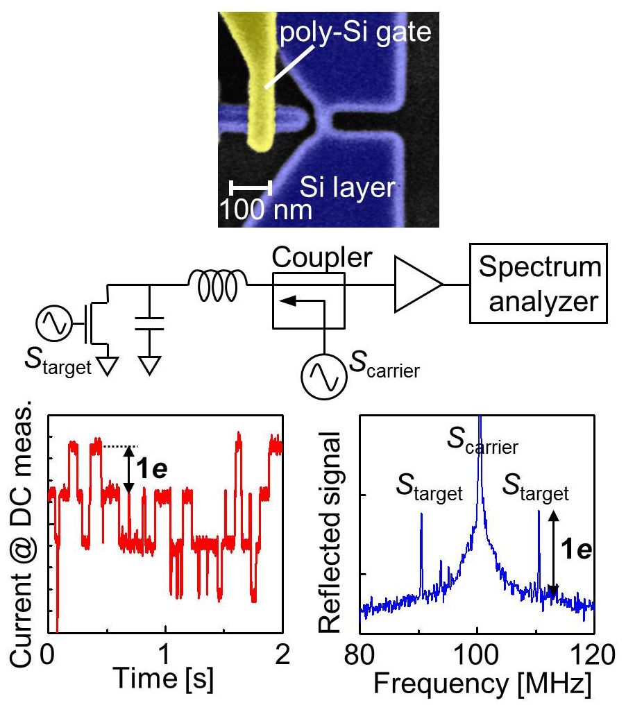 | ||
| K. Nishiguchi, H. Yamaguchi, A. Fujiwara, H. S. J. Zant, and G. A. Steele | |||
| [ABSTRACT] We demonstrate high-speed charge detection at room temperature with single-electron resolution by using a radio-frequency field-effect transistor (RF-FET). The RF-FET combines a nanometer-scale silicon FET with an impedance-matching circuit composed of an inductor and capacitor. Driving the RF-FET with a carrier signal at resonance frequency, small signals at the transistor’s gate modulate the resonance condition, which is monitored at high speed using the reflected signal. The RF-FET driven by high-power carrier signals enables a charge sensitivity of 2×10^-4 e/Hz^0.5 at readout band-width of 20 MHz. | |||
| Water Electrolysis and Energy Harvesting with Zero-Dimensional Ion-Sensitive Field-Effect Transistors | |
| Nano Lett. vol. 13, p. 3903 (2013) | |
| N. Clément, K. Nishiguchi, J. F. Dufreche, D. Guerin, A. Fujiwara, and D. Vuillaume | |
| [ABSTRACT]The relationship of the gas bubble size to the size distribution critically influences the effectiveness of electrochemical processes. Several optical and acoustical techniques have been used to characterize the size and emission frequency of bubbles. Here, we used zero-dimensional (0D) ion-sensitive field-effect transistors (ISFETs) buried under a microbath to detect the emission of individual bubbles electrically and to generate statistics on the bubble emission time. The bubble size was evaluated via a simple model of the electrolytic current. We suggest that energy lost during water electrolysis could be used to generate electric pulses at an optimal efficiency with an array of 0D ISFETs. | |
| Phonon Lasing in an Electromechanical Resonator | |
| Phys. Rev. Lett. vol. 110, p. 127202 (2013) | |
| I. Mahboob, K. Nishiguchi, A. Fujiwara, and H. Yamaguchi | |
| [ABSTRACT]An electromechanical resonator harboring an atomlike spectrum of discrete mechanical vibrations, namely, phonon modes, has been developed. A purely mechanical three-mode system becomes available in the electromechanical atom in which the energy difference of the two higher modes is resonant with a long-lived lower mode. Our measurements reveal that even an incoherent input into the higher mode results in coherent emission in the lower mode that exhibits all the hallmarks of phonon lasing in a process that is reminiscent of Brillouin lasing. | |
| Detecting signals buried in noise via nanowire transistors using stochastic resonance | |||
| Appl. Phys. Lett. vol. 101, p. 193108 (2012). | Signal detection using a transitor with small S-swing 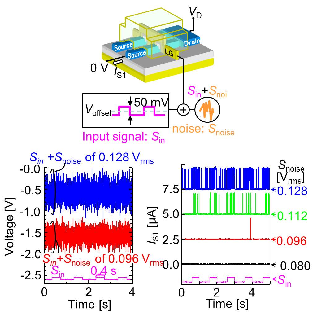 | ||
| K. Nishiguchi and A. Fujiwara | |||
| [ABSTRACT] We demonstrate stochastic resonance (SR), which takes advantage of noise to detect a weak signal, using a field-effect transistor (FET). An FET’s structure composed of a nanowire channel enables current characteristics to show strong nonlinearity, which overcomes thermal limitation, and dynamic bistability, both of which boost an effect of SR and silhouette noise from noise. Moreover, the dynamic bistability enables SR effect to be enhanced by adding common noise to multiple FETs. The FET providing such unique characteristics opens the way to use SR for practical applications. | |||
| Phonon-cavity electromechanics | |
| Nature Physics, vol. 8, pp. 387-392 (2012) | |
| I. Mahboob, K. Nishiguchi, H. Okamoto, and H. Yamaguchi | |
| [ABSTRACT]Photonic cavities have emerged as an indispensable tool to control and manipulate harmonic motion in opto/electromechanical systems. Invariably, in these systems a high-quality-factor photonic mode is parametrically coupled to a high-quality-factor mechanical oscillation mode. This entails the demanding challenges of either combining two physically distinct systems, or else optimizing the same nanostructure for both mechanical and optical properties. In contrast to these approaches, here we show that the cavity can be realized by the second oscillation mode of the same mechanical oscillator. A piezoelectric pump generates strain-induced parametric coupling between the first and the second mode at a rate that can exceed their intrinsic relaxation rate. This leads to a mechanically induced transparency in the second mode which plays the role of the phonon cavity, the emergence of parametric normal-mode splittingand the ability to cool the first mode. Thus, the mechanical oscillator can now be completely manipulated by a phonon cavity | |
| Tuneable electromechanical comb generation | |
| Appl. Phys. Lett. vol. 100, p. 113109 (2012) | |
| I. Mahboob, Q. Wilmart, K. Nishiguchi, A. Fujiwara, and H. Yamaguchi | |
| [ABSTRACT]An array of equally spaced oscillations or a comb is created within the bandwidth of the fundamental mode of an electromechanical resonator. This phenomenon utilises 2 continuous-wave (CW) pump excitations that piezoelectrically modulate the tension in the mechanical element and is seeded by a CW harmonic excitation of the first mode i.e., the signal. The resultant comb can be dynamically manipulated via the pumps and signal where the teeth separation can be tuned over 3 orders of magnitude and the comb density can be increased from just 2 teeth to nearly 10^2. (c) 2012 American Institute of Physics | |
| Wide-band idler generation in a GaAs electromechanical resonator | |
| Phys. Rev. B, vol. 84, p. 113411 (2011). | |
| I. Mahboob, Q. Wilmart, K. Nishiguchi, A. Fujiwara, and H. Yamaguchi | |
| [ABSTRACT]Periodically modulating the piezoelectrically introduced strain in an electromechanical resonator can enable the fundamental (ω0) and the first modes (ω1) to be coupled. This is explicitly demonstrated with the creation of a mechanical idler at ω1 (ω0) when a signal excitation is applied at ω0 (ω1) and a pump excitation is applied at ω0+ω1. The dynamics of the mechanical idler generation are captured by a simple phenomenological model and our experimental demonstration paves the way toward accessing the diverse functionality of nonlinear optics in an on-chip electromechanical platform. | |
| Evaluation of a Gate Capacitance in the Sub-aF Range for a Chemical Field-Effect Transistor With a Si Nanowire Channel | |
| IEEE Trans. Nanotechnology, vol. 10, p. 1172 (2011). | |
| N. Clement, K. Nishiguchi, A. Fujiwara, and D. Vuillaume | |
| [ABSTRACT]An evaluation of the gate capacitance of a field-effect transitor (FET), whose channel length and width are several ten nanometer, is a key point for sensors applications. However, experimental and precise evaluation of capacitance in the attofarad range or less has been extremely difficult. Here, we report an extraction of the capacitance down to 0.55 aF for a Si FET with a nanoscale wire channel, whose width and length are 15 and 50 nm, respectively. The extraction can be achieved by using a combination of four kinds of measurements: current characteristics modulated by double gates, random-telegraph-signal noise induced by trapping and detrapping of a single electron, dielectric polarization noise, and current characteristics showing Coulomb blockade at low temperature. The extraction of such a small gate capacitance enables us to evaluate electron mobility in a nanoscale wire by using a classical model of current characteristics of an FET. | |
| Single-Electron Stochastic Resonance Using Si Nanowire Transistors | |||
| Picked up in SPOTLIGHTS: Editors'Choice from APEX and JJAP. | |||
| Jpn. J. Appl. Phys., vol. 50, p. 06GF04 (2011). | Patern perception using stochastic resonace  | ||
| K. Nishiguchi and A. Fujiwara | |||
| [ABSTRACT] We demonstrate stochastic resonance (SR) with single electrons (SEs) using nanoscale meta-oxide-semiconductor field-effect transistors (MOSFETs). Input signal applied to a MOSFET modulates SE transport in an average manner based on nonlinear characteristics. On the other hand, an individual SE goes through the MOSFET in a completely random manner, which corresponds to shot noise. SEs transferred to a storage node are counted precisely by the other MOSFET and used as an output signal. The correlation between the input and output signals is improved by taking advantage of extrinsic noise as well as the intrinsic shot noise composed of SEs. It is confirmed that the shot-noise-assisted SR allows fast operation with a simple system. Pattern perception utilizing SR is also demonstrated. | |||
| Single-electron counting statistics of shot noise in nanowire Si metal-oxide-semiconductor field-effect transistors | |||
| Picked up in the May 23, 20011 issue of Virtual Journal of Nanoscale Science & Technology | |||
| Appl. Phys. Lett., vol. 98, p. 193502 (2011). | Time-domain analysis on shot noise 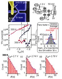 | ||
| K. Nishiguchi, Y. Ono, and A. Fujiwara | |||
| [ABSTRACT] Shot noise in the transport of single electrons in a Si metal-oxide-semiconductor field-effect transistor is monitored by real-time measurement with a high-charge-sensitivity electrometer. In the current range between zepto and attoamperes, the current characteristics are found to be divided into two regimes: a temperature-independent regime in the lower current range and a temperature-dependent one in the higher current range. A time-domain analysis reveals that, for both regimes, the single-electron transport obeys a pure Poisson process with the Fano factor’s being nearly unity, while the shot noise is suppressed with reduced Fano factors around the boundary. c 2011 American Institute of Physics | |||
| Accuracy evaluation of single-electron shuttle transfer in Si nanowire metal-oxide-semiconductor field-effect transistors | |||
| Appl. Phys. Lett., vol. 98, p. 222104 (2011). | |||
| G. Yamahata, K. Nishiguchi, and A. Fujiwara | |||
| [ABSTRACT] We report on evaluation of transfer accuracy in a single-electron turnstile using silicon nanowire metal-oxide-semiconductor field-effect transistors at 17 K. Single-electron shuttle transfer and single-shot detection of a single electron are used to detect errors of the transfer. Errors for the transfer through an electrostatically formed island are ascribed to thermal processes. We also observed single-electron transfer mediated by a trap level, which exhibits a wide current plateau and a low error rate. c 2011 American Institute of Physics | |||
| Interconnect-free parallel logic circuits in a single mechanical resonator | |||
| Nature Communications, v. 2, DOI:10.1038/ncomms1201 (2011). | |||
| I. Mahboob, E. Flurin, K. Nishiguchi, A. Fujiwara, and H. Yamaguchi | |||
| [ABSTRACT] In conventional computers, wiring between transistors is required to enable the execution of Boolean logic functions. This has resulted in processors in which billions of transistors are physically interconnected, which limits integration densities, gives rise to huge power consumption and restricts processing speeds. A method to eliminate wiring amongst transistors by condensing Boolean logic into a single active element is thus highly desirable. Here, we demonstrate a novel logic architecture using only a single electromechanical parametric resonator into which multiple channels of binary information are encoded as mechanical oscillations at different frequencies. The parametric resonator can mix these channels, resulting in new mechanical oscillation states that enable the construction of AND, OR and XOR logic gates as well as multibit logic circuits. Moreover, the mechanical logic gates and circuits can be executed simultaneously, giving rise to the prospect of a parallel logic processor in just a single mechanical resonator. | |||
| A silicon nanowire ion-sensitive field-effect transistor with elementary charge sensitivity | |||
| Appl. Phys. Lett., vol. 98, p. 014104 (2011). | |||
| N. Clement, K. Nishiguchi, J. F. Dufreche, D. Guerin, A. Fujiwara, and D. Vuillaume | |||
| [ABSTRACT] We investigate the mechanisms responsible for the low-frequency noise in liquid-gated nanoscale silicon nanowire field-effect transistors (SiNW-FETs) and show that the charge-noise level is lower than elementary charge. Our measurements also show that ionic strength of the surrounding electrolyte has a minimal effect on the overall noise. Dielectric polarization noise seems to be at the origin of the 1/f noise in our devices. The estimated spectral density of charge noise Sq = 1.6×10^-2/Hz^1/2 at 10 Hz opens the door to metrological studies with these SiNW-FETs for the electrical detection of a small number of molecules. c 2011 American Institute of Physics | |||
| Enhanced force sensitivity and noise squeezing in an electromechanical resonator coupled to a nanotransistor | |||
| Appl. Phys. Lett., vol. 97, p. 253105 (2010). | |||
| I. Mahboob, E. Flurin, K. Nishiguchi, A. Fujiwara, and H. Yamaguchi | |||
| [ABSTRACT] A nanofield-effect transistor (nano-FET) is coupled to a massive piezoelectricity based electromechanical resonator integrated with a parametric amplifier. The mechanical parametric amplifier can enhance the resonator’s displacement and the resulting electrical signal is further amplified by the nano-FET. This hybrid amplification scheme yields an increase in the mechanical displacement signal by 70 dB resulting in a force sensitivity of 200 aNHz^-1/2 at 3 K. The mechanical parametric amplifier can also squeeze the displacement noise in one oscillation phase by 5 dB enabling a factor of 4 reduction in the thermomechanical noise force level. c 2010 American Institute of Physics | |||
| One-by-one trap activation in silicon nanowire transistors | |||
| Nature Communications, v. 1, DOI:10.1038/ncomms1092 (2010). | |||
| N. Clement , K. Nishiguchi, A. Fujiwara, and D. Vuillaume | |||
| [ABSTRACT] Flicker or 1/f noise in metal-oxide-semiconductor field-effect transistors (MOSFETs) has been identified as the main source of noise at low frequency. It often originates from an ensemble of a huge number of charges becoming trapped and de-trapped. However, as a deviation from the well-known model of 1/f noise is observed for nanoscale MOSFETs, a new model is required. Here, we report the observation of one-by-one trap activation controlled by the gate voltage in a nanowire MOSFET and propose a new low-frequency-noise theory for nanoscale FETs. We show that the Coulomb repulsion between electronically charged trap sites prevents the activation of several traps simultaneously. This effect induces a noise reduction of more than one order of magnitude. It decreases when the electron density in the channel is increased due to the electrical screening of traps. These findings are technologically useful for any FET with a short and narrow channel. | |||
| Si nanowire ion-sensitive field-effect transistors with a shared floating gate | |||
| Appl. Phys. Lett., vol. 94, p. 163106 (2009). | Real-time monitoring of molecules 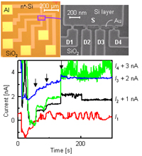 | ||
| K. Nishiguchi, N. Clement , T. Yamaguchi, and A. Fujiwara | |||
| [ABSTRACT] Ion-sensitive field-effect transistors (ISFETs) arrayed in parallel were fabricated on a silicon-on-insulator substrate. Since the nanoscale wire channels of the ISFETs are bridged with a floating gate on which molecules are preferably immobilized, signals originating from charged materials only on the floating gate can appear and can therefore be distinguished from background noise, which leads to noise-robust sensing. Additionally, the nanoscale channels provide the ISFETs with single-electron-resolution charge sensitivity as well as a reduction in background noise induced in the wider channels used as electrical leads. These features promise the detection of a small number of molecules. c 2009 American Institute of Physics | |||
| Single-electron counting statistics and its circuit application in nanoscale field-effect transistors at room temperature | |||
| Nanotechnology, vol. 20, p. 175201 (2009). | Flexible pattern recognition | ||
| K. Nishiguchi and A. Fujiwara | |||
| [ABSTRACT] A circuit utilizing single electrons is demonstrated at room temperature. Individual electrons randomly passing through the nanoscale silicon-on-insulator metal-oxide-semiconductor field-effect transistor (MOSFET) are monitored by an electrometer in real time. Such a random behavior of single electrons is used for high-quality random-number generation suitable for data processing which stochastically extracts the most preferable pattern among various ones. MOSFET-based random-number generation allows fast operation as well as high controllability, which leads to flexible extraction of the preferable pattern. | |||
| Room temperature piezoelectric displacement detection via a silicon field effect transistor | |||
| Appl. Phys. Lett., vol. 95, p. 233102 (2009). | |||
| I. Mahboob, K. Nishiguchi, A. Fujiwara, and H. Yamaguchi | |||
| [ABSTRACT] An electromechanical oscillator embedded with a two dimensional electron gas is capacitively coupled to a silicon field effect transistor (Si-FET). The piezovoltage induced by the mechanical motion modulates the current passing through the Si-FET enabling the electromechanical oscillator’s position to be monitored. When the Si-FET is biased at its optimal point, the motion induced piezovoltage can be amplified resulting in a displacement sensitivity of 6×10^-12mHz-1/2 for a 131 kHz GaAs resonator which is among the highest recorded for an all-electrical room temperature detection scheme. c 2009 American Institute of Physics | |||
| Stochastic data processing circuit based on single electrons using nanoscale field-effect transistors | |||
| Picked up in the February 25, 2008 issue of Virtual Journal
of Nanoscale Science & Technology. Picked up in News and Views of the May 8, 2008 online issue of Nature. | |||
| Appl. Phys. Lett., vol. 92, p. 062105 (2008). | Flexible logic circuit | ||
| K. Nishiguchi, Y. Ono, A. Fujiwara, H. Inokawa, and Y. Takahashi | |||
| [ABSTRACT] A circuit utilizing single electrons is demonstrated at room temperature using a silicon-on-insulator metal-oxide-semiconductor field-effect transistor (MOSFET). Individual electrons randomly passing through the nanoscale MOSFET, which are the origin of shot noise, are monitored by an electrometer in real time. This random behavior of single electrons is used as a random number for a stochastic associative memory for image-pattern matching, in which the most preferable pattern is extracted with the largest probability. The use of electron transport in the MOSFET provides high controllability of the randomness as well as fast generation of random numbers. The present result promises single-electron applications using nanoscale MOSFETs. c 2008 American Institute of Physics | |||
| Single-Electron-Resolution Electrometer Based on Field-Effect Transistor | |||
| Picked up in the December 15, 2008 issue of Virtual Journal of Nanoscale Science & Technology | |||
| Jpn. J. Appl. Phys., vol. 47, pp. 8305-8310 (2008). | Single-electron detection at room temperature 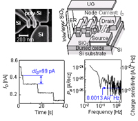 | ||
| K. Nishiguchi, C. Koechlin, Y. Ono, A. Fujiwara, H. Inokawa, and H. Yamaguchi | |||
| [ABSTRACT] An electrometer based on field-effect transistors (FETs) was fabricated on a silicon-on-insulator substrate (SOI). The electrometer has a nanometer-scale small channel and a capacitively coupled node, where single electrons are stored. We discuss the dependence of the charge sensitivity of the electrometer on its structure and on its operation condition and gives guides for achieving the higher charge sensitivity. The device optimization based on this dependence allows the demonstration of the electrometer with extremely high charge sensitivity, 0.0013 e/√Hz at 1 Hz, at room temperature. | |||
| Infrared detection with silicon nano field-effect transistors | |||
| Picked up in the June 11, 2007 issue of Virtual Journal
of Nanoscale Science and Technology Picked up in the August, 2007 issue of Photonics Spectra Picked up in the July, 2007 issue of Laser Focus World | |||
| Appl. Phys. Lett., vol. 90, p. 223108 (2007). | Infrared detection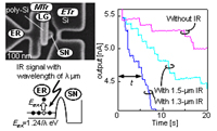 | ||
| K. Nishiguchi, A. Fujiwara, Y. Ono, H. Inokawa, and Y. Takahashi | |||
| [ABSTRACT] The authors fabricated nanoscale silicon metal-oxide-semiconductor field-effect transistors (MOSFETs) to detect an infrared (IR) signal at room temperature. The IR signal excites conduction-band electrons in an undoped channel of a MOSFET and some of them are injected through an energy barrier into a storage node (SN) electrically formed by the MOSFET. Small signals, originating from electrons, stored in the SN are detected by an electrometer with a single-electron resolution. Additionally, the MOSFET controls the number and energy of electrons injected into the SN. This enables electrical control of the sensitivity and cutoff wavelengths of IR signals, suggesting the possibility of highly functional IR sensors. c 2007 American Institute of Physics | |||
| Identification of single and coupled acceptors in silicon nano-field-effect transistors | |||
| Appl. Phys. Lett., vol. 12, 263513 (2007) | |||
| M. A. H. Khalafalla, Y. Ono, K. Nishiguchi, and A. Fujiwara. | |||
| [ABSTRACT] We performed dopant mediated hole transport measurements to identify the depth position of individual boron acceptors and investigate two-acceptor coupling in silicon-on-insulator nanoscale field-effect transistors at a temperature of 6 K. The depth position is qualitatively obtained from the analysis of the acceptor-to-gate capacitances. We also observe signatures of a two-acceptor capacitive coupling in the characteristics of the conductance versus the front and back gate voltages. c 2007 American Institute of Physics | |||
| Transfer and detection of single electrons using metal-oxide-semiconductor field-effect transistors | |||
| IEICE Trans. Electron., vol. E90-C, p. 943 (2007). | |||
| W. Zhang, K. Nishiguchi, Y. Ono, A. Fujiwara, H. Yamaguchi, H. Inokawa, Y. Takahashi, and N. J. Wu. | |||
| [ABSTRACT] A single-electron turnstile and electrometer circuit was fabricated on a silicon-on-insulator substrate. The turnstile, which is operated by opening and closing two metal-oxide-semiconductor field-effect transistors (MOSFETs) alternately, allows current quantization at 20 K due to single-electron transfer. Another MOSFET is placed at the drain side of the turnstile to form an electron storage island. Therefore, one-by-one electron entrance into the storage island from the turnstile can be detected as an abrupt change in the current of the electrometer, which is placed near the storage island and electrically coupled to it. The correspondence between the quantized current and the single-electron counting was confirmed. | |||
| Room-temperature-operating data processing circuit based on single-electron transfer and detection with metal-oxide-semiconductor field-effect transistor technology | |||
| Picked up in the May 15, 2006 issue of Virtual Journal
of Nanoscale Science & Technology Picked up in the June 29, 2006 online issue of Nature Nanotechnology. | |||
| Appl. Phys. Lett., vol. 88, p. 183101 (2006). | Digital-Analog Converter using single electrons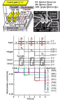 | ||
| K. Nishiguchi, A. Fujiwara, Y. Ono, H. Inokawa, and Y. Takahashi | |||
| [ABSTRACT] A single-electron-based circuit, in which electrons are transferred one by one with a turnstile and subsequently detected with a high-charge-sensitivity electrometer, was fabricated on a silicon-on-insulator substrate. The turnstile, which is operated by opening and closing two metal-oxide-semiconductor field-effect transistors alternately, allows single-electron transfer at room temperature owing to electric-field-assisted shrinkage of the single-electron box. It also achieves fast single-electron transfer (less than 10 ns) and extremely long retention (more than 10^4 s). We have applied these features to a multilevel memory and a time-division weighted sum circuit for a digital-to-analog converter. c 2006 American Institute of Physicsys | |||
| Manipulation and detection of single electrons for future information processing | |||
| J. Appl. Phys., vol. 97, p. 031101 (2005). | |||
| Y. Ono, A. Fujiwara, K. Nishiguchi, H. Inokawa, and Y. Takahashi | |||
| [ABSTRACT] vThe ultimate goal of future information processing might be the realization of a circuit in which one bit is represented by a single electron. Such a challenging circuit would comprise elemental devices whose tasks are to drag, transfer, and detect single electrons. In achieving these tasks, the Coulomb blockade, which occurs in tiny conducting materials, plays an important role. This paper describes the current status of research on such single-charge-control devices from the viewpoints of circuit applications. c 2005 American Institute of Physics | |||
| Multilevel memory using an electrically formed single-electron box | |||
| Picked up in August 23, 2004 issue of Virtual Journal of Nanoscale Science & Technology. | |||
| Appl. Phys. Lett., vol. 85, pp. 1277-1279 (2004). | Multileval memory represented by single electrons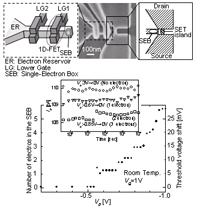 | ||
| K. Nishiguchi, H. Inokawa, Y. Ono, A. Fujiwara, and Y. Takahashi | |||
| [ABSTRACT] A multilevel dynamic random-access memory using a single-electron box (SEB) and single-electron transistor (SET) is fabricated on a silicon-on-insulator substrate. A one-dimensional field-effect transistor (FET), which is connected to the SEB, modulates a barrier potential to precisely control the number of electrons one by one in the SEB by means of the Coulomb-blockade phenomenon. At room temperature and 26 K, we demonstrate a multilevel memory, in which each interval between the levels is given by a single electron, by using the SET electrometer coupled capacitively to the SEB. The control of stored electrons by the FET assures long-retention time and high-speed write/erase operation. | |||
| Multilevel memory using single-electron turnstile | |||
| Electron. Lett., vol. 40, pp. 229-230 (2004). | Single-electron transfer and detection 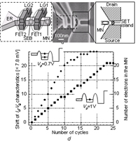 | ||
| K. Nishiguchi, H. Inokawa, Y. Ono, A. Fujiwara, and Y. Takahashi | |||
| [ABSTRACT] A multilevel single-electron memory has been successfully demonstrated. Two fine gates with phase-shifted pulse voltages modulate potential barriers in a one-dimensional Si channel to transfer electrons one by one into a memory node, and the number of electrons in the node is sensed by a single-electron transistor. | |||