| |
Nanodevice's group Advanced Applied Physical Science Laboratory NTT Basic Research Laboratories |
| |
Nanodevice's group Advanced Applied Physical Science Laboratory NTT Basic Research Laboratories |
| First-Principles Investigation of the Valley Splitting of Si Quantum Slabs | |||
| Physica Status Solidi. B. p. 2400531 (2024) DOI: 10.1002/pssb.202400531 | |||
| T. Hayashi, H. Kageshima, Y. Tokura, J. Noborisaka, and K. Nishiguchi | |||
| [ABSTRACT] First-principles calculations based on density functional theory are performed on silicon (Si) quantum slabs to investigate the valley splitting of the lowest sub-bands at the Γ point in the conduction band. The calculations show that strong strain in the [110] direction of the slab largely enhances the valley splitting, which may be related to the giant valley splitting observed in a device consisting of silicon-on-insulator and buried oxide layers. The relation between the valley splitting and the atomic configuration of the slabs is also examined. | |||
| Noise-to-energy conversion in a nanometer-scale dot observed with electron counting statistics | |||
| Appl. Phys. Lett. vol. 122, 213502 (2023). | |||
| K. Chida, A. Fujiwara, and K. Nishiguchi | |||
| [ABSTRACT] We converted Gaussian-distributed voltage noise applied to an electron reservoir into the non-equilibrium free energy of a nanometer-scale dot connected to the reservoir via an energy barrier. Counting statistics of single-electron motion into and out of the dot through the energy barrier allows us to quantitatively analyze the energy transported into the dot as well as changes in the internal energy and effective temperature of the dot in this noise-induced non-equilibrium steady state (NESS). By analyzing the transition rates of electrons moving into and out of the dot, we confirmed that the rectification effect caused by the asymmetry with respect to the direction of electron motion is the origin of the increase in the internal energy of the dot. The information on energy transport in a nanometer-scale dot in the noise-induced NESS obtained in this study with electron counting statistics clarifies the relationship between the non-equilibrium dynamics of a nanodevice and noise applied to it. This study provides us with the means to evaluate device operation using noise as a resource. | |||
| Planar cold cathode based on a multilayer-graphene/SiO2/Si heterodevice | |||
| Appl. Phys. Exp. vol. 9, p. 105101 (2016) | Electron emission from multilayer graphene 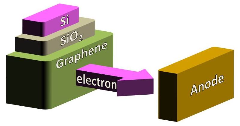 | ||
| K. Nishiguchi, D. Yoshizumi, Y. Sekine, K. Furukawa, A. Fujiwara, and M. Nagase | |||
| [ABSTRACT] We have fabricated a planar cold cathode based on a multilayer (ML)-graphene/SiO2/Si heterostructure. When voltage is applied between the ML graphene and Si layer, electrons tunnel from the Si layer to the ML-graphene through the SiO2. During this tunneling event, electrons repeatedly gain and lose energy in the SiO2 owing to the electric field and scattering, respectively. Electrons whose energy is larger than the work function of the ML-graphene are emitted from its surface to a vacuum. The thinness of the ML-graphene reduces the energy loss of electrons in it and thus improves electron emission characteristics. | |||
| Observing the semiconducting band-gap alignment of MoS2 layers of different atomic thicknesses using a MoS2/SiO2/Si heterojunction tunnel diode | |||
| Selected for the Featured Article and cover image | |||
| Appl. Phys. Lett. vol. 107, 053101 (2015). | Tunnel diode 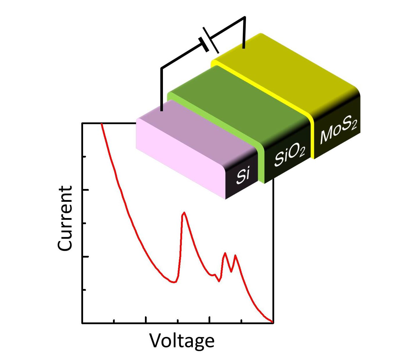 | ||
| K. Nishiguchi, A. Castellanos-Gomez, H. Yamaguchi, A. Fujiwara, H.S. J. van der Zant, G. A. Steele | |||
| [ABSTRACT] We demonstrate a tunnel diode composed of a vertical MoS2/SiO2/Si heterostructure. A MoS2 flake consisting four areas of different thickness functions as a gate terminal of a silicon field-effect transistor. A thin gate oxide allows tunneling current to flow between the n-type MoS2 layers and p-type Si channel. The tunneling-current characteristics show multiple negative differential resistance features, which we interpret as an indication of different conduction-band alignments of the MoS2 layers of different thickness. The presented tunnel device can be also used as a hy-brid-heterostructure device combining the advantages of two-dimensional materials with those of silicon transistors. | |||
| Single-Electron Stochastic Resonance Using Si Nanowire Transistors | |||
| Picked up in SPOTLIGHTS: Editors'Choice from APEX and JJAP. | |||
| Jpn. J. Appl. Phys., vol. 50, p. 06GF04 (2011). | Patern perception using stochastic resonace  | ||
| K. Nishiguchi and A. Fujiwara | |||
| [ABSTRACT] We demonstrate stochastic resonance (SR) with single electrons (SEs) using nanoscale metal-oxide-semiconductor field-effect transistors (MOSFETs). Input signal applied to a MOSFET modulates SE transport in an average manner based on nonlinear characteristics. On the other hand, an individual SE goes through the MOSFET in a completely random manner, which corresponds to shot noise. SEs transferred to a storage node are counted precisely by the other MOSFET and used as an output signal. The correlation between the input and output signals is improved by taking advantage of extrinsic noise as well as the intrinsic shot noise composed of SEs. It is confirmed that the shot-noise-assisted SR allows fast operation with a simple system. Pattern perception utilizing SR is also demonstrated. | |||
| Si nanowire ion-sensitive field-effect transistors with a shared floating gate | |||
| Appl. Phys. Lett., vol. 94, p. 163106 (2009). | Real-time monitoring of molecules  | ||
| K. Nishiguchi, N. Clement , T. Yamaguchi, and A. Fujiwara | |||
| [ABSTRACT] Ion-sensitive field-effect transistors (ISFETs) arrayed in parallel were fabricated on a silicon-on-insulator substrate. Since the nanoscale wire channels of the ISFETs are bridged with a floating gate on which molecules are preferably immobilized, signals originating from charged materials only on the floating gate can appear and can therefore be distinguished from background noise, which leads to noise-robust sensing. Additionally, the nanoscale channels provide the ISFETs with single-electron-resolution charge sensitivity as well as a reduction in background noise induced in the wider channels used as electrical leads. These features promise the detection of a small number of molecules. c 2009 American Institute of Physics | |||
| Single-electron counting statistics and its circuit application in nanoscale field-effect transistors at room temperature | |||
| Nanotechnology, vol. 20, p. 175201 (2009). | Flexible pattern recognition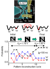 | ||
| K. Nishiguchi and A. Fujiwara | |||
| [ABSTRACT] A circuit utilizing single electrons is demonstrated at room temperature. Individual electrons randomly passing through the nanoscale silicon-on-insulator metal-oxide-semiconductor field-effect transistor (MOSFET) are monitored by an electrometer in real time. Such a random behavior of single electrons is used for high-quality random-number generation suitable for data processing which stochastically extracts the most preferable pattern among various ones. MOSFET-based random-number generation allows fast operation as well as high controllability, which leads to flexible extraction of the preferable pattern. | |||
| Stochastic data processing circuit based on single electrons using nanoscale field-effect transistors | |||
| Picked up in the February 25, 2008 issue of Virtual Journal
of Nanoscale Science & Technology. Picked up in News and Views of the May 8, 2008 online issue of Nature. | |||
| Appl. Phys. Lett., vol. 92, p. 062105 (2008). | Flexible logic circuit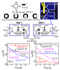 | ||
| K. Nishiguchi, Y. Ono, A. Fujiwara, H. Inokawa, and Y. Takahashi | |||
| [ABSTRACT] A circuit utilizing single electrons is demonstrated at room temperature using a silicon-on-insulator metal-oxide-semiconductor field-effect transistor (MOSFET). Individual electrons randomly passing through the nanoscale MOSFET, which are the origin of shot noise, are monitored by an electrometer in real time. This random behavior of single electrons is used as a random number for a stochastic associative memory for image-pattern matching, in which the most preferable pattern is extracted with the largest probability. The use of electron transport in the MOSFET provides high controllability of the randomness as well as fast generation of random numbers. The present result promises single-electron applications using nanoscale MOSFETs. c 2008 American Institute of Physics | |||
| Infrared detection with silicon nano field-effect transistors | |||
| Picked up in the June 11, 2007 issue of Virtual Journal
of Nanoscale Science and Technology Picked up in the August, 2007 issue of Photonics Spectra Picked up in the July, 2007 issue of Laser Focus World | |||
| Appl. Phys. Lett., vol. 90, p. 223108 (2007). | Infrared detection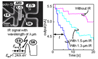 | ||
| K. Nishiguchi, A. Fujiwara, Y. Ono, H. Inokawa, and Y. Takahashi | |||
| [ABSTRACT] The authors fabricated nanoscale silicon metal-oxide-semiconductor field-effect transistors (MOSFETs) to detect an infrared (IR) signal at room temperature. The IR signal excites conduction-band electrons in an undoped channel of a MOSFET and some of them are injected through an energy barrier into a storage node (SN) electrically formed by the MOSFET. Small signals, originating from electrons, stored in the SN are detected by an electrometer with a single-electron resolution. Additionally, the MOSFET controls the number and energy of electrons injected into the SN. This enables electrical control of the sensitivity and cutoff wavelengths of IR signals, suggesting the possibility of highly functional IR sensors. c 2007 American Institute of Physics | |||
| Room-temperature-operating data processing circuit based on single-electron transfer and detection with metal-oxide-semiconductor field-effect transistor technology | |||
| Picked up in the May 15, 2006 issue of Virtual Journal
of Nanoscale Science & Technology Picked up in the June 29, 2006 online issue of Nature Nanotechnology. | |||
| Appl. Phys. Lett., vol. 88, p. 183101 (2006). | Digital-Analog Converter using single electrons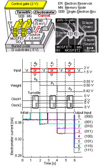 | ||
| K. Nishiguchi, A. Fujiwara, Y. Ono, H. Inokawa, and Y. Takahashi | |||
| [ABSTRACT] A single-electron-based circuit, in which electrons are transferred one by one with a turnstile and subsequently detected with a high-charge-sensitivity electrometer, was fabricated on a silicon-on-insulator substrate. The turnstile, which is operated by opening and closing two metal-oxide-semiconductor field-effect transistors alternately, allows single-electron transfer at room temperature owing to electric-field-assisted shrinkage of the single-electron box. It also achieves fast single-electron transfer (less than 10 ns) and extremely long retention (more than 10^4 s). We have applied these features to a multilevel memory and a time-division weighted sum circuit for a digital-to-analog converter. c 2006 American Institute of Physicsys | |||
| Multifunctional Boolean Logic Using Single-Electron Transistors | |||
| IEICE Trans. Electron., vol. E87-C, pp. 1809-1817 (2004). | Multileval memory represented by single electrons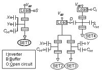 | ||
| K. Nishiguchi, H. Inokawa, Y. Ono, A. Fujiwara, and Y. Takahashi | |||
| [ABSTRACT] A multifunctional Boolean logic circuit composed of single-electron transistors (SETs) was fabricated and its operation demonstrated. The functions of Boolean logic can be changed by the half-period phase shift of the Coulomb-blockade (CB) oscillation of some SETs in the circuit, and an automatic control based on a feedback process is used to attain an exact shift. The amount of charges in the memory node (MN), which is capacitively coupled to the SET, controls the phase of the CB oscillation, and the output signal of the SET controls the amount of charge in the MN during the feedback process. This feedback process automatically adjusts SET output characteristics in such a way that it is used for the multifunctional Boolean logic. We experimentally demonstrated the automatic phase control and examined the speed of the feedback process by SPICE circuit simulation combined with a compact analytical SET model. The simulation revealed that programming time could be of the order of a few ten nanoseconds, thereby promising high-speed switching of the functions of the multifunctional Boolean logic circuit. | |||
| Multilevel memory using an electrically formed single-electron box | |||
| Picked up in August 23, 2004 issue of Virtual Journal of Nanoscale Science & Technology. | |||
| Appl. Phys. Lett., vol. 85, pp. 1277-1279 (2004). | Multileval memory represented by single electrons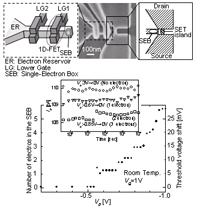 | ||
| K. Nishiguchi, H. Inokawa, Y. Ono, A. Fujiwara, and Y. Takahashi | |||
| [ABSTRACT] A multilevel dynamic random-access memory using a single-electron box (SEB) and single-electron transistor (SET) is fabricated on a silicon-on-insulator substrate. A one-dimensional field-effect transistor (FET), which is connected to the SEB, modulates a barrier potential to precisely control the number of electrons one by one in the SEB by means of the Coulomb-blockade phenomenon. At room temperature and 26 K, we demonstrate a multilevel memory, in which each interval between the levels is given by a single electron, by using the SET electrometer coupled capacitively to the SEB. The control of stored electrons by the FET assures long-retention time and high-speed write/erase operation. | |||
| Multilevel memory using single-electron turnstile | |||
| Electron. Lett., vol. 40, pp. 229-230 (2004). | Single-electron transfer and detection 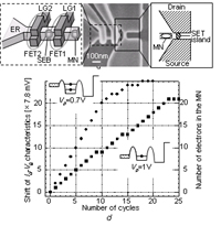 | ||
| K. Nishiguchi, H. Inokawa, Y. Ono, A. Fujiwara, and Y. Takahashi | |||
| [ABSTRACT] A multilevel single-electron memory has been successfully demonstrated. Two fine gates with phase-shifted pulse voltages modulate potential barriers in a one-dimensional Si channel to transfer electrons one by one into a memory node, and the number of electrons in the node is sensed by a single-electron transistor. | |||